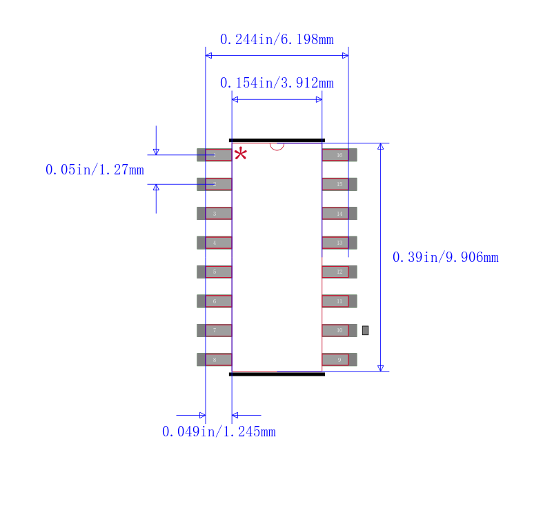
MC74LVX259DG
数据手册.pdf8位可寻址锁存器/带LSTTL兼容输入1 -OF- 8解码器CMOS逻辑电平转换器 8-Bit Addressable Latch/1-of-8 Decoder CMOS Logic Level Shifter with LSTTL−Compatible Inputs
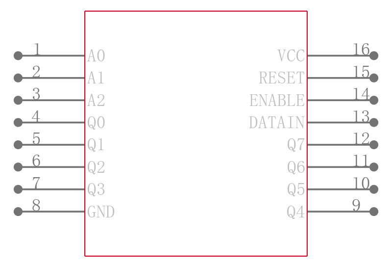
The MC74LVX259 is an 8-bit Addressable Latch fabricated with silicon gate CMOS technology.The internal circuit is composed of three stages, including a buffer output which provides high noise immunity and stable output.The LVX259 is designed for general purpose storage applications in digital systems. The device has four modes of operation as shown in the mode selection table.. In the addressable latch mode, the data on Data In is written into the addressed latch. The addressed latch follows the data input with all non-addressed latches remaining in their previous states. In the memory mode, all latches remain in their previous state and are unaffected by the Data or Address inputs. In the one-of-eight decoding or demultiplexing mode, the addressed output follows the state of Data In with all other outputs in the LOW state. In the Reset mode, all outputs are LOW and unaffected by the address and data inputs. When operating the LVX259 as an addressable latch, changing more than one bit of the address ould impose a transient wrong address. Therefore, this should only be done while in thememory mode. The MC74LVX259 input structure provides protection when voltages up to 7 V are applied, regardless of the supply voltage. This allows the MC74LVX259 to be used to interface 5 V circuits to 3 V circuits.
Features
---
|
- .
- High Speed: tPD = 7.0 ns Typ at VCC = 3.3 V
- .
- Low Power Dissipation: ICC = 2 µA Max at TA = 25°C
- .
- High Noise Immunity: VNIH = VNIL = 28% VCC
- .
- CMOS-Compatible Outputs: VOH > 0.8 VCC ; VOL < 0.1 VCC @Load
- .
- Power Down Protection Provided on Inputs and Outputs
- .
- Balanced Propagation Delays
- .
- Pin and Function Compatible with Other Standard Logic Families
- .
- Latchup Performance Exceeds 300 mA
- .
- ESD Performance: HBM > 2000 V; Machine Model > 200 V
- .
- Pb-Free Packages are Available*