MC100LVEP210FAG
数据手册.pdfMC100LVEP210 系列 3 GHz 3.8 V 1:5 双 差分ECL/PECL/HSTL 时钟驱动器
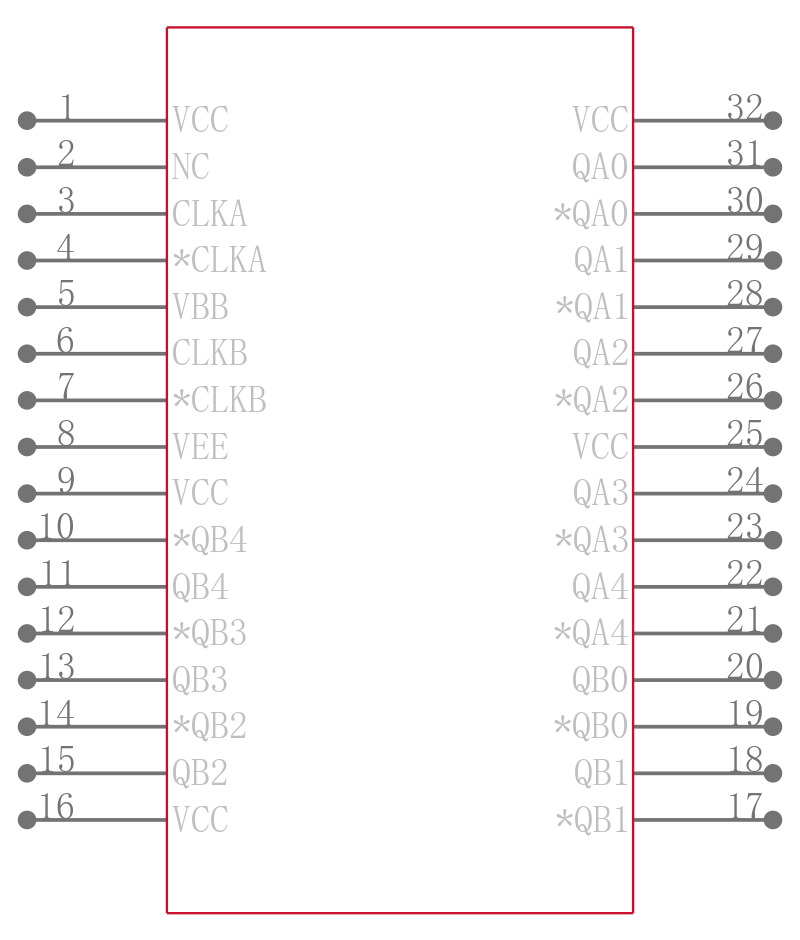
The MC100LVEP210 is a low skew 1-to-5 dual differential driver, designed with clock distribution in mind. The ECL/PECL input signals can be either differential or single ended if the V output is used. The signal is fanned out to 5 identical differential outputs. HSTL inputs can be used when the EP210 is operating in PECL mode.The LVEP210 specifically guarantees low output-to-output skew.Optimal design, layout, and processing minimize skew within a device and from device to device. To ensure the tight skew specification is realized, both sides of the differential output need to be terminated identically into 50 ohms even if only one output is being used. If an output pair is unused, both outputs may be left open unterminated without affecting skew.The MC100LVEP210, as with most other ECL devices, can be operated from a positive V supply in PECL mode. This allows the LVEP210 to be used for high performance clock distribution in +3.3 V or +2.5 V systems. Single-ended CLK input operation is limited to a VDesigners can take advantage of the LVEP210"s performance to distribute low skew clocks across the backplane or the board. In a PECL environment, series or Thevenin line terminations are typically used as they require no additional power supplies. For more information on using PECL, designers should refer to Application Note AN1406/D.
Features
---
|
- .
- 85 ps Typical Device-to-Device Skew
- .
- 20 ps Typical Output-to-Output Skew
- .
- VBBOutput
- .
- Jitter Less than 1 ps RMS
- .
- 350 ps Typical Propagation Delay
- .
- Maximum Frequency >3 Ghz
- .
- The 100 Series Contains Temperature Compensation
- .
- PECL and HSTL Mode Operating Range: VCC = 2.375 V to 3.8 V with VEE = 0 V
- .
- NECL Mode Operating Range: VCC = 0 V with VEE = -2.375 V to -3.8 V
- .
- Open Input Default State
- .
- LVDS Input Compatible