MC14043BDG
数据手册.pdfON SEMICONDUCTOR MC14043BDG 芯片, 4000系列 CMOS逻辑器件
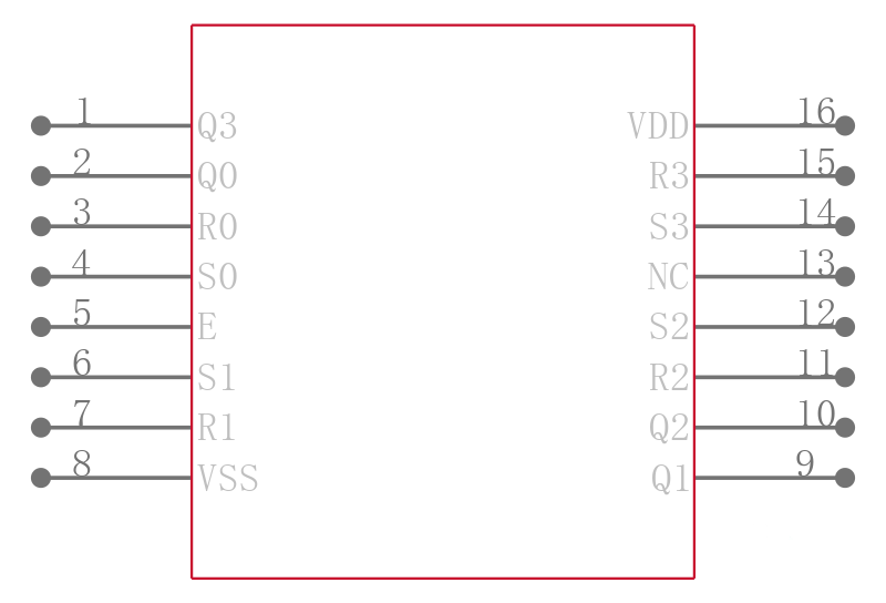
The is a quad R-S Latch constructed with MOS P-channel and N-channel enhancement mode devices in a single monolithic structure. Each latch has an independent Q output and set and reset inputs. The Q outputs are gated through three-state buffers having a common enable input. The outputs are enabled with a logical 1 or high on the enable input, a logical 0 or low disconnects the latch from the Q outputs, resulting in an open circuit at the Q outputs. The outputs are capable of driving two low-power TTL loads or one low-power Schottky TTL load over the rated temperature range. This device contains protection circuitry to guard against damage due to high static voltages or electric fields.
- .
- Double diode input protection
- .
- Three-state outputs with common enable
Precautions must be taken to avoid applications of any voltage higher than maximum rated voltages to this high-impedance circuit.