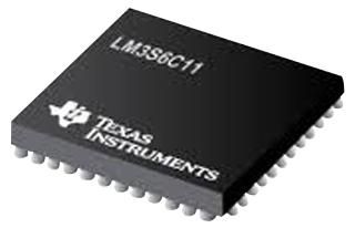
LM3S6911-IBZ50-A2
的Stellaris LM3S6911微控制器 Stellaris LM3S6911 Microcontroller
Architectural Overview
The Stellaris® family of microcontrollers—the first ARM® Cortex™-M3 based controllers—brings high-performance 32-bit computing to cost-sensitive embedded microcontroller applications. These pioneering parts deliver customers 32-bit performance at a cost equivalent to legacy 8- and 16-bit devices, all in a package with a small footprint.
Product Features
The LM3S6911 microcontroller includes the following product features:
■ 32-Bit RISC Performance
– 32-bit ARM® Cortex™-M3 v7M architecture optimized for small-footprint embedded applications
– System timer SysTick, providing a simple, 24-bit clear-on-write, decrementing, wrap-on-zero counter with a flexible control mechanism
– Thumb®-compatible Thumb-2-only instruction set processor core for high code density
– 50-MHz operation
– Hardware-division and single-cycle-multiplication
– Integrated Nested Vectored Interrupt Controller NVIC providing deterministic interrupt
handling
– 30 interrupts with eight priority levels
– Memory protection unit MPU, providing a privileged mode for protected operating system
functionality
– Unaligned data access, enabling data to be efficiently packed into memory
– Atomic bit manipulation bit-banding, delivering maximum memory utilization and streamlined
peripheral control
■ ARM® Cortex™-M3 Processor Core
– Compact core.
– Thumb-2 instruction set, delivering the high-performance expected of an ARM core in the memory size usually associated with 8- and 16-bit devices; typically in the range of a few kilobytes of memory for microcontroller class applications.
– Rapid application execution through Harvard architecture characterized by separate buses for instruction and data.
– Exceptional interrupt handling, by implementing the register manipulations required for handling an interrupt in hardware.
– Deterministic, fast interrupt processing: always 12 cycles, or just 6 cycles with tail-chaining
– Memory protection unit MPU to provide a privileged mode of operation for complex applications.
– Migration from the ARM7™ processor family for better performance and power efficiency.
– Full-featured debug solution
• Serial Wire JTAG Debug Port SWJ-DP
• Flash Patch and Breakpoint FPB unit for implementing breakpoints
• Data Watchpoint and Trigger DWT unit for implementing watchpoints, trigger resources, and system profiling
• Instrumentation Trace Macrocell ITM for support of printf style debugging
• Trace Port Interface Unit TPIU for bridging to a Trace Port Analyzer
– Optimized for single-cycle flash usage
– Three sleep modes with clock gating for low power
– Single-cycle multiply instruction and hardware divide
– Atomic operations
– ARM Thumb2 mixed 16-/32-bit instruction set
– 1.25 DMIPS/MHz
■ JTAG
– IEEE 1149.1-1990 compatible Test Access Port TAP controller
– Four-bit Instruction Register IR chain for storing JTAG instructions
– IEEE standard instructions: BYPASS, IDCODE, SAMPLE/PRELOAD, EXTEST and INTEST
– ARM additional instructions: APACC, DPACC and ABORT
– Integrated ARM Serial Wire Debug SWD
■ Hibernation
– System power control using discrete external regulator
– Dedicated pin for waking from an external signal
– Low-battery detection, signaling, and interrupt generation
– 32-bit real-time clock RTC
– Two 32-bit RTC match registers for timed wake-up and interrupt generation
– Clock source from a 32.768-kHz external oscillator or a 4.194304-MHz crystal
– RTC predivider trim for making fine adjustments to the clock rate
– 64 32-bit words of non-volatile memory
– Programmable interrupts for RTC match, external wake, and low battery events
■ Internal Memory
– 256 KB single-cycle flash
• User-managed flash block protection on a 2-KB block basis
• User-managed flash data programming
• User-defined and managed flash-protection block
– 64 KB single-cycle SRAM
■ GPIOs
– 10-46 GPIOs, depending on configuration
– 5-V-tolerant in input configuration
– Fast toggle capable of a change every two clock cycles
– Programmable control for GPIO interrupts
• Interrupt generation masking
• Edge-triggered on rising, falling, or both
• Level-sensitive on High or Low values
– Bit masking in both read and write operations through address lines
– Pins configured as digital inputs are Schmitt-triggered.
– Programmable control for GPIO pad configuration
• Weak pull-up or pull-down resistors
• 2-mA, 4-mA, and 8-mA pad drive for digital communication; up to four pads can be configured with an 18-mA pad drive for high-current applications
• Slew rate control for the 8-mA drive
• Open drain enables
• Digital input enables