ADP2138ACBZ-1.2-R7
数据手册.pdf降压型 Vin=2.3V~5.5V Vout=1.2V 800mA
Product Details
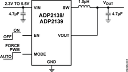
The ADP2138 and ADP2139 are high efficiency, low quiescent current, synchronous step-down dc-to-dc converters. The ADP2139 has the additional feature of an internal discharge switch. The total solution requires only three tiny external components. When the MODE pin is set high, the buck regulator operates in forced PWM mode, which provides low peak-to-peak ripple for power supply noise sensitive loads at the expense of light load efficiency. When the MODE pin is set low, the buck regulator automatically switches operating modes, depending on the load current level. At higher output loads, the buck regulator operates in PWM mode. When the load current falls below a predefined threshold, the regulator operates in power save mode PSM, improving light load efficiency.
The ADP2138/ADP2139 operate on input voltages of 2.3 V to 5.5 V, which allows for single lithium or lithium polymer cell, multiple alkaline or NiMH cell, PCMCIA, USB, and other standard power sources. The maximum load current of 800 mA is achievable across the input voltage range.
The ADP2138/ADP2139 are available in fixed output voltages of 3.3 V, 3.0 V, 2.8 V, 2.5 V, 1.8 V, 1.5 V, 1.2 V, 1.0 V, and 0.8 V. All versions include an internal power switch and synchronous rect-ifier for minimal external part count and high efficiency. The ADP2138/ADP2139 have internal soft start and they are internally compensated. During logic controlled shutdown, the input is disconnected from the output and the ADP2138/ADP2139 draw 0.2 μA typical from the input source.
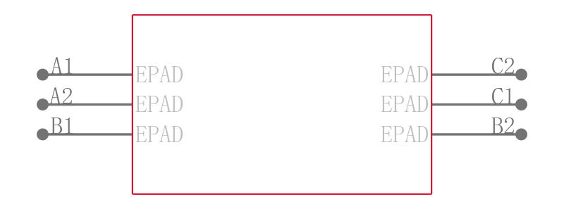
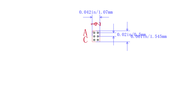
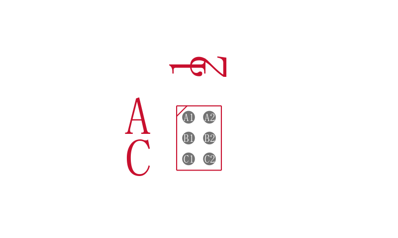
Other key features include undervoltage lockout to prevent deep battery discharge, and soft start to prevent input current over-shoot at startup. The ADP2138/ADP2139 are available in a 6-ball wafer level chip scale package WLCSP.
**Applications**
- .
- PDAs and palmtop computers
- .
- Wireless handsets
- .
- Digital audio, portable media players
- .
- Digital cameras, GPS navigation units
### Features and Benefits
- .
- Input voltage: 2.3 V to 5.5 V
- .
- Peak efficiency: 95%
- .
- 3 MHz fixed frequency operation
- .
- Typical quiescent current: 24 μA
- .
- Very small solution size
6-lead, 1 mm × 1.5 mm WLCSP package
- .
- Fast load and line transient response
- .
- 100% duty cycle low dropout mode
- .
- Internal synchronous rectifier, compensation, and soft start
- .
- Current overload and thermal shutdown protections
- .
- Ultralow shutdown current: 0.2 μA typical
- .
- Forced PWM and automatic PWM/PSM modes
- .
- Supported by simPower Design Tool