ADC3444IRTQ25
TEXAS INSTRUMENTS ADC3444IRTQ25 模数转换器, 4通道, 14 bit, 125 MSPS, 单, 1.7 V, 1.9 V, VQFN
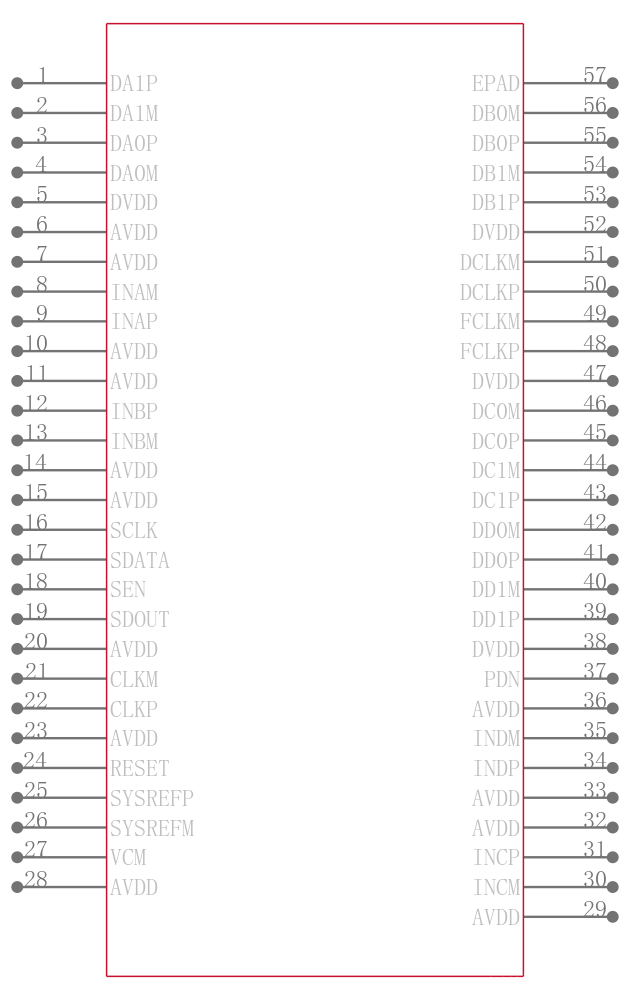
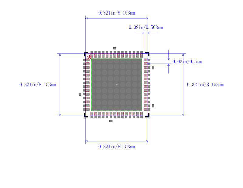
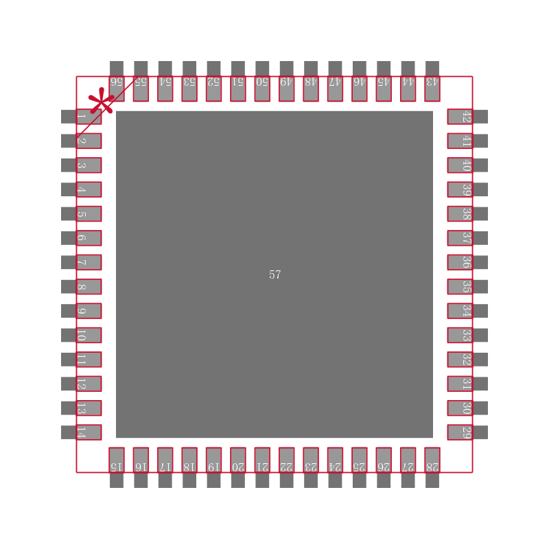
The is a quad-channel, 14bit analogue to digital converter in 56 pin VQFN package. The device is designed specifically to support demanding, high input frequency signals with large dynamic range requirements. An input clock divider allows more flexibility for system clock architecture design while the SYSREF input enables complete system synchronization. It supports serial LVDS interface in order to reduce the number of interface lines, thus allowing for high system integration density. The serial LVDS interface is two-wire, where each ADC data are serialized and output over two LVDS pairs. An internal phase locked loop PLL multiplies the incoming ADC sampling clock to derive the bit clock that is used to serialize the 14bit output data from each channel. In addition to the serial data streams, the frame and bit clocks are also transmitted as LVDS outputs. It is used in multi-carrier, multi-mode cellular base stations, munitions guidance, radar and smart antenna arrays.
- .
- Supply voltage range from 1.7V to 1.9V
- .
- Operating temperature range from -40°C to 85°C
- .
- Maximum ADC clock frequency of 125MSPS
- .
- SNR = 72.4dBFS, SFDR = 87dBc at fIN = 70MHz
- .
- Maximum analogue and digital supply current is 162mA and 145mA
- .
- Maximum total power dissipation of 475mW
- .
- Maximum global power down dissipation is 17mW
- .
- Standby power down dissipation is 103mW
ESD sensitive device, take proper precaution while handling the device.