FDN359AN
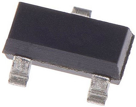
数据手册.pdfFAIRCHILD SEMICONDUCTOR FDN359AN... 场效应管, MOSFET, N沟道, 30V, 2.7A, SSOT
最大源漏极电压Vds Drain-Source Voltage| 30V \---|--- 最大栅源极电压Vgs± Gate-Source Voltage| 20V 最大漏极电流Id Drain Current| 2.7A 源漏极导通电阻ΩRds DΩ/Ohmain-SouΩ/Ohmce On-State Ω/Ohmesistance| 0.046Ω/Ohm @2.7A,10V 开启电压Vgs(th) Gate-Source Threshold Voltage| 1-3V 耗散功率Pd Power Dissipation| 500mW/0.5W Description & Applications| N-Channel Logic Level PowerTrench TM MOSFET General Description This N-Channel Logic Level MOSFET is produced using Semiconductor"s advanced PowerTrench process that has been especially tailored to minimize on-state resistance and yet maintain uperior switching performance. These devices are well suited for low voltage and battery powered applications where low in-line power loss and fast switching are required. 2.7 A, 30 V. RDSON = 0.046 W @ VGS = 10 V RDSON = 0.060 W @ VGS = 4.5 V. Very fast switching. Low gate charge 5nC typical. High power version of industry standard SOT-23 package. Identical pin out to SOT-23 with 30% higher power handling capability. 描述与应用| N沟道逻辑电平的PowerTrench TM MOSFET 概述 这N沟道逻辑电平MOSFET产生 采用飞兆半导体先进的 PowerTrench进程,已特别定制 尽量减少对通态电阻,但维持优越的开关性能。 这些器件非常适用于低电压,电池供电应用中低线的功率 损耗和快速开关是必需的。 开关速度非常快。 低栅极电荷(典5NC) 高功率版本的行业标包相同的引脚SOT-23高出30% 功率处理能力