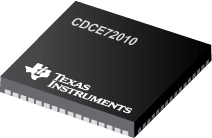
CDCE72010
10 路输出低抖动时钟同步器和抖动消除器
The is a high-performance, low phase noise, and low skew clock synchronizer that synchronizes a VCXO Voltage Controlled Crystal Oscillator or VCO Voltage Controlled Oscillator frequency to one of two reference clocks. The clock path is fully programmable providing the user with a high degree of flexibility. The following relationship applies to the dividers:
Frequency VCXO_IN or AUX_IN / Frequency PRI_REF or SEC_REF = P- .
- N/R*M
The VCXO_IN clock operates up to 1.5GHz through the selection of external VCXO and loop filter components. The PLL loop bandwidth and damping factor can be adjusted to meet different system requirements.
The CDCE72010 can lock to one of two reference clock inputs PRI_REF and SEC_REF and supports frequency hold-over mode for fail-safe and system redundancy. The outputs of the CDCE72010 are user definable and can be any combination of up to 10 LVPECL/LVDS outputs or up to 20 LVCMOS outputs. The built-in synchronization latches ensure that all outputs are synchronized for very low output skew.
All device settings, including output signaling, divider value selection, input selection, and many more, are programmable with the SPI 4-wire Serial Peripheral Interface. The SPI allows individual control of the device settings.
The device operates in a 3.3V environment and is characterized for operation from –40°C to +85°C.
The CDCE72010 is available in a 64-pin lead-free “green” plastic quad flatpack package with enhanced bottom thermal pad for heat dissipation. The Texas Instruments package designator is RGC S-PQFP-N64.
- .
- High Performance LVPECL, LVDS, LVCMOS PLL Clock Synchronizer
- .
- Two Reference Clock Inputs Primary and Secondary Clock for Redundancy
Support with Manual or Automatic Selection
- .
- Accepts Two Differential Input LVPECL or LVDS References up to 500MHz
or Two LVCMOS Inputs up to 250MHz as PLL Reference
- .
- VCXO_IN Clock is Synchronized to One of Two Reference Clocks
- .
- VCXO_IN Frequencies up to 1.5GHz LVPECL
800MHz for LVDS and
250MHz for LVCMOS Level Signaling
- .
- Outputs Can be a Combination of LVPECL, LVDS, and LVCMOS
Up to 10 Differential LVPECL or LVDS Outputs or up to
20 LVCMOS Outputs, Output 9 can be Converted to an
Auxiliary Input as a 2nd VCXO.
- .
- Output Divider is Selectable to Divide by 1, 2, 3, 4, 5, 6, 8, 10,
12, 16, 18, 20, 24, 28, 30, 32, 36, 40, 42, 48, 50, 56, 60, 64, 70,
or 80 On Each Output Individually up to Eight Dividers. Except for
Output 0 and 9, Output 0 Follows Output 1 Divider and Output 9
Follows Output 8 Divider
- .
- SPI Controllable Device Setting
- .
- Individual Output Enable Control via SPI Interface
- .
- Integrated On-Chip Non-Volatile Memory EEPROM to Store Settings
without the Need to Apply High Voltage to the Device
- .
- Optional Configuration Pins to Select Between Two Default Settings
Stored in EEPROM
- .
- Efficient Jitter Cleaning from Low PLL Loop Bandwidth
- .
- Very Low Phase Noise PLL Core
- .
- Programmable Phase Offset Input Reference to Outputs
- .
- Wide Charge-Pump Current Range From 200µA to 3mA
- .
- Presets Charge-Pump to VCC_CP/2 for Fast Center-Frequency
Setting of VCXO, Controlled Via the SPI Bus
- .
- SERDES Startup Mode Depending on VCXO Range
- .
- Auxiliary Input: Output 9 can Serve as 2nd VCXO Input to Drive
All Outputs or to Serve as PLL Feedback Signal
- .
- RESET or HOLD Input Pin to Serve as Reset or Hold Functions
- .
- REFERENCE SELECT for Manual Select Between Primary and Secondary
Reference Clocks
- .
- POWER DOWN PD to Put Device in Standby Mode
- .
- Analog and Digital PLL Lock Indicator
- .
- Internally Generated VBB Bias Voltages for Single-Ended Input Signals
- .
- Frequency Hold-Over Mode Activated by HOLD Pin or SPI Bus to Improve
Fail-Safe Operation
- .
- Input to All Outputs Skew Control
- .
- Individual Skew Control for Each Output with Each Output Divider
- .
- Packaged in a QFN-64 Package
- .
- ESD Protection Exceeds 2kV HBM
- .
- Industrial Temperature Range of –40°C to 85°

