CY7C1320CV18-267BZXC
数据手册.pdf18兆位的DDR - II SRAM的2字突发架构 18-Mbit DDR-II SRAM 2-Word Burst Architecture
Functional Description
The CY7C1316CV18, CY7C1916CV18, CY7C1318CV18, and CY7C1320CV18 are 1.8V Synchronous Pipelined SRAMs equipped with DDR-II architecture. The DDR-II consists of an SRAM core with advanced synchronous peripheral circuitry and a one-bit burst counter. Addresses for read and write are latched on alternate rising edges of the input K clock.
Features
■18-Mbit density 2M x 8, 2M x 9, 1M x 18, 512K x 36
■267 MHz clock for high bandwidth
■2-word burst for reducing address bus frequency
■Double Data Rate DDR interfaces data transferred at 534 MHz at 267 MHz
■Synchronous internally self-timed writes
■DDR-II operates with 1.5 cycle read latency when the DLL is enabled
■Operates similar to a DDR-I device with 1 cycle read latency in DLL off mode
■1.8V core power supply with HSTL inputs and outputs
■Variable drive HSTL output buffers
■Expanded HSTL output voltage 1.4V–VDD
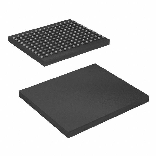
■Available in 165-Ball FBGA package 13 x 15 x 1.4 mm
■Offered in both Pb-free and non Pb-free packages
■JTAG 1149.1 compatible test access port
■Delay Lock Loop DLL for accurate data placement