AD585SCHIPS
数据手册.pdfComplete Monolithic SHA Circuit
Product Details
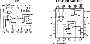
The AD585 is a complete monolithic sample-and-hold circuit consisting of a high performance operational amplifier in series with an ultralow leakage analog switch and a FET input integrating amplifier. An internal holding capacitor and matched applications resistors have been provided for high precision and applications flexibility.
The performance of the AD585 makes it ideal for high speed 10- and 12-bit data acquisition systems, where fast acquisition time, low sample-to-hold offset, and low droop are critical. The AD585 can acquire a signal to ±0.01% in 3 µs maximum, and then hold that signal with a maximum sample-to-hold offset of 3 mV and less than 1 mV/ms droop, using the on-chip hold capacitor. If lower droop is required, it is possible to add a larger external hold capacitor.
The high speed analog switch used in the AD585 exhibits aperture jitter of 0.5 ns, enabling the device to sample full scale 20 V peak-to-peak signals at frequencies up to 78 kHz with 12-bit precision.
The AD585 can be used with any user-defined feedback net-work to provide any desired gain in the sample mode. On-chip precision thin-film resistors can be used to provide gains of +1, -1, or +2. Output impedance in the hold mode is sufficiently low to maintain an accurate output signal even when driving the dynamic load presented by a successive-approximation A/D converter. However, the output is protected against damage from accidental short circuits.
The control signal for the HOLD command can be either active high or active low. The differential HOLD signal is compatible with all logic families, if a suitable reference level is provided. An on-chip TTL reference level is provided for TTL compatibility.
The AD585 is available in three performance grades. The JP grade is specified for the 0°C to +70°C commercial temperature range and packaged in a 20-pin PLCC. The AQ grade is specified for the -25°C to +85°C industrial temperature range and is packaged in a 14-pin cerdip. The SQ and SE grades are specified for the -55°C to +125°C military temperature range and are packaged in a 14-pin cerdip and 20-pin LCC.
### Features and Benefits
- .
- 3.0 ms Acquisition Time to 60.01% max
- .
- Low Droop Rate: 1.0 mV/ms max
- .
- Sample/Hold Offset Step: 3 mV max
- .
- Aperture Jitter: 0.5 ns
- .
- Extended Temperature Range: –55°C to +125°C
- .
- Internal Hold Capacitor
- .
- Internal Application Resistors
- .
- See datasheet for additional features