HMC7043LP7FE
数据手册.pdfANALOG DEVICES HMC7043LP7FE 芯片, 扇出缓冲器, 3.2GHZ, 14输出, LFCSP-48 新
Product Details
The HMC7043 is designed to meet the requirements of multicarrier GSM and LTE base station designs, and offers a wide range of clock management and distribution features to simplify baseband and radio card clock tree designs.
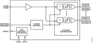
The HMC7043 provides 14 low noise and configurable outputs to offer flexibility in interfacing with many different components in a base transceiver station BTS system, such as data converters, local oscillators, transmit/receive modules, field programmable gate arrays FPGAs, and digital front-end ASICs. The HMC7043 can generate up to seven DCLK and SYSREF clock pairs per the JESD204B interface requirements.
The system designer can generate a lower number of DCLK and SYSREF pairs, and configure the remaining output signal paths for independent phase and frequency. Both the DCLK and SYSREF clock outputs can be configured to support different signaling standards, including CML, LVDS, LVPECL, and LVCMOS, and different bias conditions to adjust for varying board insertion losses.
One of the unique features of the HMC7043 is the independent flexible phase management of each of the 14 channels. All 14 channels feature both frequency and phase adjustment. The outputs can also be programmed for 50 Ω or 100 Ω internal and external termination options.
The HMC7043 device features an RF SYNC feature that synchronizes multiple HMC7043 devices deterministically, that is, ensures that all clock outputs start with the same edge. This operation is achieved by rephrasing the nested HMC7043 or SYSREF control unit/divider, deterministically, and then restarting the output dividers with this new phase.
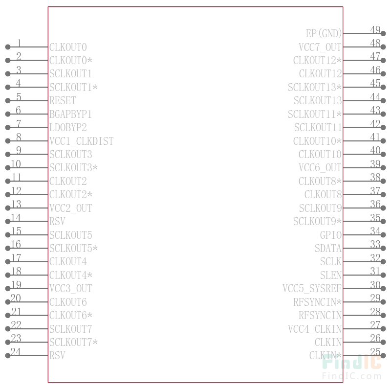
The HMC7043 is offered in a 48-lead, 7 mm × 7 mm LFCSP package with an exposed pad connected to ground.
Applications
- .
- JESD204B clock generation
- .
- Cellular infrastructure multicarrier GSM, LTE, W-CDMA
- .
- Data converter clocking
- .
- Phase array reference distribution
- .
- Microwave baseband cards
### Features and Benefits
- .
- JEDEC JESD204B support
- .
- Low additive jitter: <15 fs rms at 2457.6 MHz 12 kHz to 20 MHz
- .
- Very low noise floor: −155.2 dBc/Hz at 983.04 MHz
- .
- Up to 14 LVDS, LVPECL, or CML type device clocks DCLKs
- .
- Maximum CLKOUTx/CLKOUTx and SCLKOUTx/SCLKOUTx frequency of 3200 MHz
- .
- JESD204B-compatible system reference SYSREF pulses
- .
- 25 ps analog and ½ clock input cycle digital delay independently programmable on each of 14 clock output channels
- .
- SPI-programmable adjustable noise floor vs. power consumption
- .
- SYSREF valid interrupt to simplify JESD204B synchronization
- .
- Supports deterministic synchronization of multiple HMC7043 devices
- .
- RFSYNC pin or SPI-controlled SYNC trigger for output synchronization of JESD204B
- .
- GPIO alarm/status indicator to determine the health of the system
- .
- Clock input to support up to 6 GHz
- .
- On-board regulator for excellent PSRR
- .
- 48-lead, 7 mm × 7 mm LFCSP package