HMC6832ALP5LETR
数据手册.pdfClock Fanout Buffer 8Out 16Pin LFCSP EP T/R
Product Details
The HMC6832 is an input selectable, 2:8 differential fanout buffer designed for low noise clock distribution. The IN_SEL control pin selects one of the two differential inputs. This input is then buffered to all eight differential outputs. The low jitter outputs of the HMC6832 lead to synchronized low noise switching of downstream circuits, such as mixers, analog-todigital converters ADCs/digital-to-analog converters DACs, or serializer/deserializer SERDES devices. The device is capable of low voltage, positive emitter-coupled logic LVPECL or low voltage differential signaling LVDS configurations by pulling the CONFIG pin low for LVPECL or high or open internally pulled high for pseudo LVDS.
**Product Highlights**
1. Multiple Output Configurations.
The CONFIG pin allows the user to select LVPECL or LVDS output termination.
2. Multiple Supply Voltage Operation.
The HMC6832 operates at 2.5 V or 3.3 V for LVPECL terminations 2.5 V only for LVDS.
3. Low Noise.
The HMC6832 noise is low, typically from −168 dBc/Hz to −162 dBc/Hz up to 3000 MHz.
4. Low Propagation Delay.
The HMC6832 displays a low delay, less than 207 ps, typical. Channel skew is also low, ±5 ps, typical.
5. Low Core Current.
The HMC6832 has a low core current of 56 mA, typical.
**Applications**
- .
- SONET, Fibre Channel, GigE clock distribution
- .
- ADC/DAC clock distribution
- .
- Low skew and jitter clocks
- .
- Wireless/wired communications
- .
- Level translation
- .
- High performance instrumentation
- .
- Medical imaging
- .
- Single-ended to differential conversions
### Features and Benefits
- .
- Ultralow noise floor: −165.9 dBc/Hz or −165.2 dBc/Hz LVPECL or LVDS at 2000 MHz
- .
- Configurable to LVPECL or pseudo LVDS outputs
- .
- 2.5 V or 3.3 V LVPECL operation LVDS 2.5 V only
- .
- Wideband: 10 MHz to 3500 MHz operating frequency range
- .
- Flexible input interface
- .
- LVPECL, LVDS, CML, and CMOS compatible
- .
- AC or dc coupling
- .
- On-chip 50 kΩ pull-up/pull-down resistors to VDD and GND
- .
- Multiple output drivers
- .
- Up to 8 differential or 16 single-ended LVPECL or LVDS outputs
- .
- Low speed digital control via the IN_SEL and CONFIG pins
- .
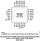
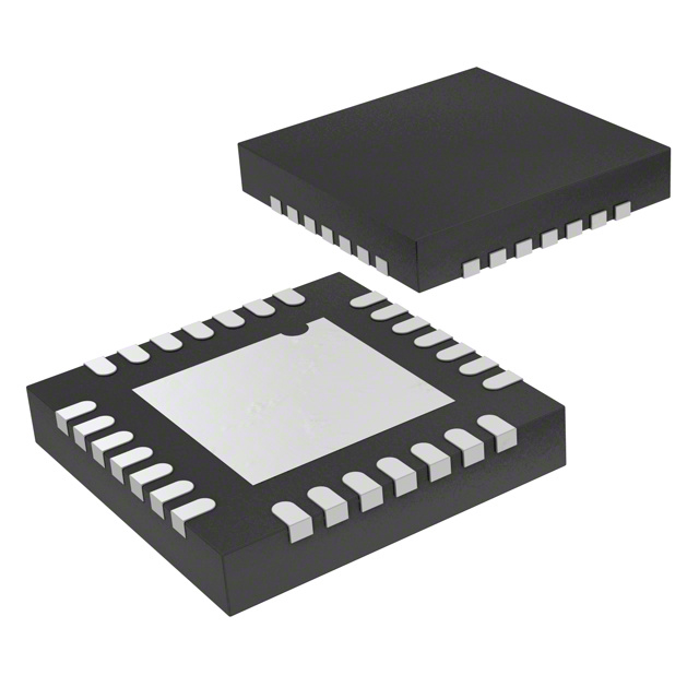
- 28-lead, 5 mm × 5 mm, LFCSP package, 25 mm2