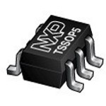
74LVC1G79GW,125
数据手册.pdf
NXP
恩智浦
主动器件
NXP 74LVC1G79GW,125 触发器, 非反相, 正沿, D, 200 MHz, 50 mA, TSSOP, 5 引脚
The 74LVC1G79GW is a single positive-edge triggered D-type Flip-flop features that the information on the data input is transferred to the Q-output on the low-to-high transition of the clock pulse. The D-input must be stable one set-up time prior to the low-to-high clock transition for predictable operation. Inputs can be driven from either 3.3 or 5V devices. This feature allows the use of this device in a mixed 3.3 and 5V environment. This device is fully specified for partial power-down applications using IOFF. The IOFF circuitry disables the output, preventing the damaging backflow current through the device when it is powered down.
- .
- High noise immunity
- .
- CMOS low power consumption
- .
- Latch-up performance exceeds 250mA
- .
- Direct interface with TTL levels
- .
- ±24mA Output drive current

