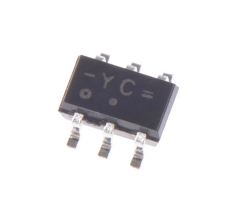
74LVC1G57GW
数据手册.pdfNXP 74LVC1G57GW 多功能逻辑门, LVC系列, 可配置, 3输入, 32 mA, 1.65V至5.5V, SOT-363-6
The is a low-power Configurable Multiple-function Gate. The output state is determined by eight patterns of 3-bit input. The user can choose the logic functions AND or, NAND, NOR, XNOR, inverter and buffer. All inputs can be connected to VCC or GND. Inputs can be driven from either 3.3V or 5V devices. This feature allows the use of this device in a mixed 3.3V and 5V environment. This device is fully specified for partial power-down applications using IOFF. The IOFF circuitry disables the output, preventing the damaging backflow current through the device when it is powered down. All inputs A, B and C are Schmitt-trigger inputs. They are capable of transforming slowly changing input signals into sharply defined, jitter-free output signals.
- .
- High noise immunity
- .
- Complies with JEDEC standard - JESD8-7, JESD8-5 and JESD8-B/JESD36
- .
- ESD protection - HBM JESD22-A114F exceeds 2000V, MM JESD22-A115-A exceeds 200V
- .
- ±24mA Output drive VCC = 3V
- .
- CMOS low power consumption
- .
- Latch-up performance exceeds 250mA
- .
- Direct interface with TTL levels
- .
- Inputs accept voltages up to 5V

