74LVC1G08GW,125
数据手册.pdf
NXP
恩智浦
主动器件
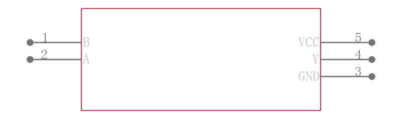
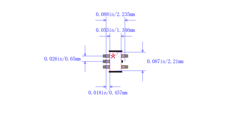
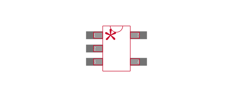
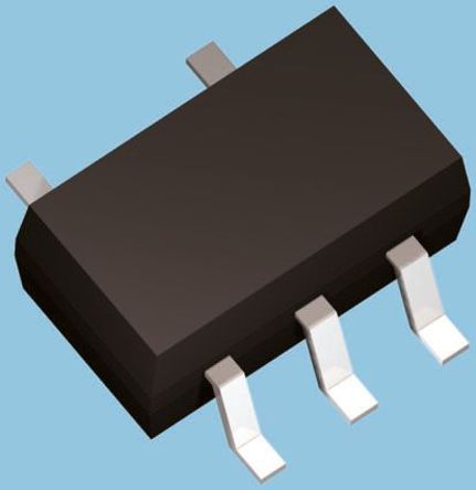
NXP 74LVC1G08GW,125. 芯片, 与门, 1输入, TSSOP-5
The 74LVC1G08GW is a single 2-input AND Gate with inputs can be driven from either 3.3V or 5V devices. This feature allows the use of these devices as translators in mixed 3.3V and 5V applications. Schmitt-trigger action at all inputs makes the circuit tolerant of slower input rise and fall time. This device is fully specified for partial power-down applications using IOFF. The IOFF circuitry disables the output, preventing the damaging backflow current through the device when it is powered down.
- .
- High noise immunity
- .
- Complies with JEDEC standard - JESD8-7, JESD8-5 and JESD8-B/JESD36
- .
- ±24mA Output drive VCC = 3V
- .
- CMOS low power consumption
- .
- Latch-up performance exceeds 250mA
- .
- Direct interface with TTL levels
- .
- Inputs accept voltages up to 5V
- .
- ESD protection - HBM JESD22-A114F exceeds 2000V, MM JESD22-A115-A exceeds 200V