74LVC1G19GW,125
数据手册.pdf
NXP
恩智浦
电子元器件分类
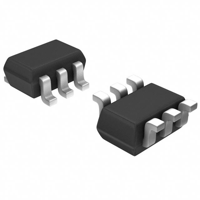
NXP 74LVC1G19GW,125 芯片, 解码器/信号分离器, 1:2, SC-88-6
The 74LVC1G19GW is a 1-of-2 Decoder/Demultiplexer with a common output enable. This device buffers the data on input A and passes it to the outputs 1Y true and 2Y complement when the enable E\\ input signal is low. Inputs can be driven from either 3.3 or 5V devices. These features allow the use of these devices in a mixed 3.3 and 5V environment. This device is fully specified for partial power-down applications using IOFF. The IOFF circuitry disables the output, preventing the damaging backflow current through the device when it is powered down.
- .
- High noise immunity
- .
- CMOS low power consumption
- .
- Latch-up performance exceeds 250mA
- .
- Direct interface with TTL levels
- .
- ±24mA Output drive current
- .
- 5V Tolerant inputs for interfacing with 5V logic