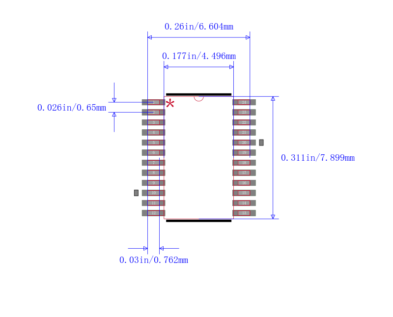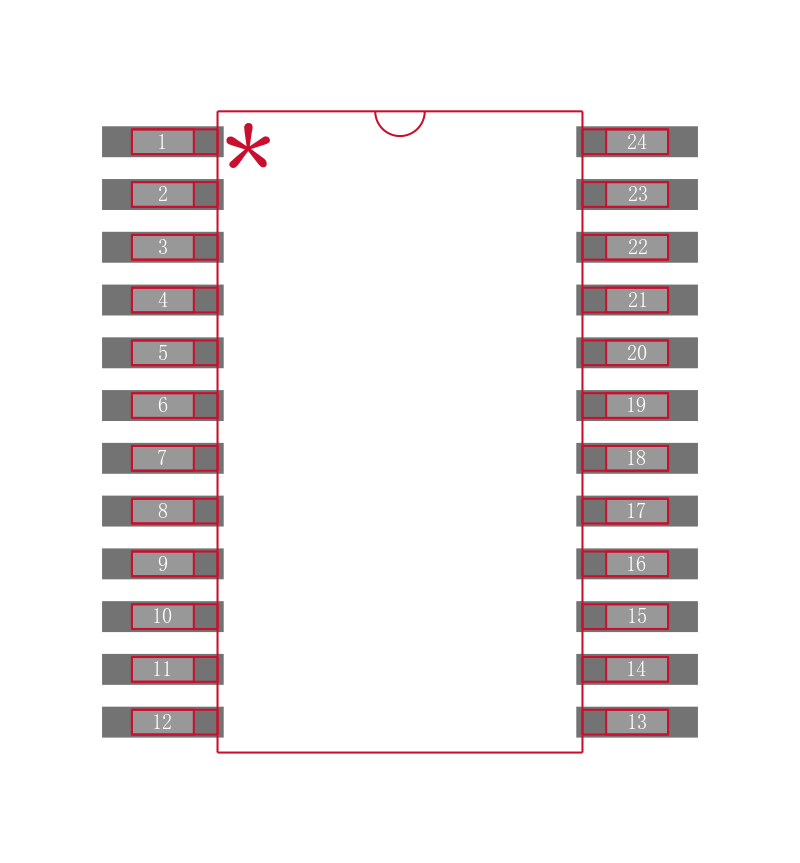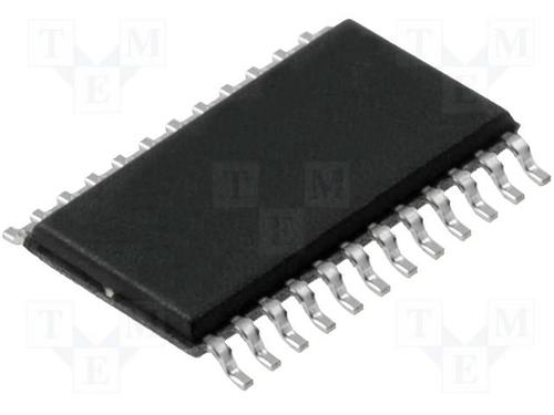
74LVC4245APW
数据手册.pdfNXP 74LVC4245APW 收发器, 转换, 3态, 1.5V至3.6V, 1.5V至5.5V, TSSOP-24
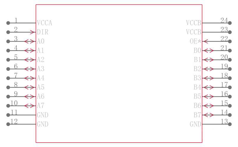
The is an octal dual supply Translating Transceiver featuring non-inverting 3-state bus compatible outputs in both send and receive directions. It is designed to interface between a 3 and 5V bus in a mixed 3 and 5V supply environment. The device features an output enable input pin OE for easy cascading and a send/receive input pin DIR for direction control. Pin OE controls the outputs so that the buses are effectively isolated. In suspend mode, when VCCA is zero, there will be no current flow from one supply to the other supply. The A-outputs must be set 3-state and the voltage on the A-bus must be smaller than Vdiode typical 0.7V.
- .
- 5V Tolerant inputs/outputs, for interfacing with 5V logic
- .
- CMOS low-power consumption
- .
- Direct interface with TTL levels
- .
- ±20µA Input leakage current and off-state output current
- .
- 40µA Supply current
- .
- Complies with JEDEC standard no. JESD8B/JESD36
ESD sensitive device, take proper precaution while handling the device.