5962-88513012A
数据手册.pdfOP Amp Single GP 20V 20Pin LCC
Product Details
The OP-42 is a fast precision JFET-input operational amplifier. Similar in speed to the OP-17, the OP-42 offers a symmetric 58V/µs slew rate and is internally compensated for unity-gain operation. OP-42 speed is achieved with a supply current of less than 6mA. Unity gain stability, a wide full-power bandwidth of 900kHz, and a fast settling-time of 800ns to 0.01% make the OP-42 an ideal output amplifier for fast digital-to-analog converters. Equal attention was given to both speed and precision in the OP-42 design.
Its tight 750µV maximum input offset voltage combined with well-controlled drift of less than 10µV/%C eliminates the need for external nulling in many circuits. The common-mode rejection of the 88dB minimum over a ±11 V input voltage range is exceptional for a high-speed amplifier. High CMR combined with a minimum 500V/mV gain into 10kohm load ensure excellent linearity in both noninverting and inverting gain configurations. The low input bias and offset currents provided by the JFET input stage suit the OP-42 for use in high-speed sample and hold circuits, peak detectors, and log amplifiers. Excellent radiation hardness characteristics make the OP-42 ideal for military and aerospace applications.
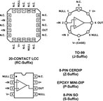
The OP-42 conforms to the standard 741 pinout with nulling to V-. The OP-42 upgrades the performance of circuits using the AD544, AD611, AD711, and LF400 by direct replacement. In circuits without nulling, the OP-42 offers an upgrade for designs using the OP-16, OP-17, LT1022, LT1056, and HA2510.
### Features and Benefits
FAST
- .
- Slew Rate: 50 V/µs Min
- .
- Settling Time 0.01%: 1 µs Max
- .
- Gain Bandwidth Product: 10 MHz Typ
- .
- Excellent Radiation Hardness
PRECISE
- .
- Common Mode Rejection: 88 dB Min
- .
- Open Loop Gain: 500 V/mV Min
- .
- Offset Voltage: 750 µV Max
- .
- Bias Current: 200 pA Max
- .
- Available in Die Form