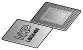
MPC8270CVVQLDA
数据手册.pdfNXP MPC8270CVVQLDA 芯片, 微控制器, 32位, POWER, 333MHZ, TBGA-480
Overview
Introducing the next generation of PowerQUICC® II™ processors: the MPC8270, MPC8275 and MPC8280.
Utilizing Our HiPerMOS7 0.13-micron process technology, the next generation PowerQUICC II family offers a range of performance, feature enhancements and package options with lower power requirements. Ideal for wired and wireless infrastructure communications processing tasks, enhancements to the PowerQUICC II family offer system designers a high degree of integrated features and functionality and a compelling, proven architecture.
The next generation of PowerQUICC II processors is an optimum solution for integrated control and forwarding plane processing in high-end communications and networking equipment -- such as routers, DSLAMs, remote access concentrators, telecom switching equipment and cellular base stations. Combining extensive layer 2 functionality with control plane processing, Our PowerQUICC II processors include a high-performance embedded 603e™ core built on Power Architecture technology, and a powerful RISC-based Communications Processor Module CPM. The CPM off-loads peripheral tasks from the embedded Power Architecture core and provides support for multiple communications protocols including 10/100Mbps Ethernet, 155Mbps ATM and 256 HDLC channels. And, of course, the next generation PowerQUICC II devices retain full software compatibility with the PowerQUICC II family.
**A range of performance and package options**
Taking advantage of the 0.13-micron process, the next generation of PowerQUICC II devices offers significant performance increases and power savings over the current generation PowerQUICC II devices, with speeds of up to 450MHz and 300MHz in the core and CPM respectively at less than 2 watts. The new processors continue to enhance the PowerQUICC architecture"s industry-leading ATM support, offering up to 2 UTOPIA ports with support for up to 31 PHYs per interface -- ideal for high-density DSLAM line cards.
The next generation of PowerQUICC II solutions also delivers support for USB, an on-target addition for high performance SOHO and CPE networking equipment. And unlike most other integrated communications processors in the market, the PowerQUICC architecture integrates two processing cores to handle specific tasks: the core built on Power Architecture technology and the RISC-based CPM -- enabling a balanced approach for systems by handling both high-level tasks and low-level communications all in one integrated device.
MoreLess
## Features
**MPC8270ZQ/VR Features**
* 603e core with 16K inst and 16K data caches
* 64-bit 60x bus, 32-bit PCI/local bus
* 128K ROM, 32K IRAM, 32K DPRAM
* Three FCCs for 10/100 Ethernet
* 128 HDLC channels, 4 TDMs
* 4 SCCs, 2 SMCs, SPI, I2C
* Memory controller built from SDRAM, UPM, GPCM machines
* New features -- USB, RMII
* Performance
* 266 MHz CPU, 200 MHz CPM, 66 MHz bus
* ~ 1W @ full performance, 1.5V
* Technology
* HIP7AP .13 micron, 3.3V I/O, 1.5V Core
* 516 PBGA, 27x27mm, 1mm ball pitch
* ZQ package has lead-bearing spheres
* VR package is lead-free
**MPC8270ZU 480 TBGA Features**
* 64-bit 60x bus, 32-bit PCI bus
* 333 MHz CPU, 250 MHz CPM, 83 MHz bus
* 450 MHz CPU, 300 MHz CPM, 100 MHz bus
* Less than 2W @ full performance, 1.5V
* HIP7AP, 3.3V I/O, 1.5V Core
* 480 TBGA, 37.5x37.5mm, 1.27mm ball pitch
## Features
* 480 TBGA, 37.5x37.5mm, 1.27mm ball pitchComparison Table
### MPC8280 Family
| 8270VR| 8270| 8275VR| 8280
\---|---|---|---|---
**SMCs** | 2 | 2 | 2 | 2
**Multichannel HDLC** | 128 | 128 | 128 | 256
**FCCs** | 3 | 3 | 3 | 3
**UTOPIA ATM** | 0 | 0 | 2 | 2
**USB** | 1 | 1 | 1 | 1
**Package** | 516 PBGA | 480 TBGA | 516 PBGA | 480 TBGA
**IMA/TC Functionality** | NO | NO | NO | YES
**MII/RMII Fast Ethernet** | 3 | 3 | 3 | 3
**SCCs** | 4 | 4 | 4 | 4
**60x/Memory Bus** | 66 | 83/100 | 66 | 83/100
**CPM** | 166 | 250/300 | 166 | 250/300
**CPU** | 266 | 333/450 | 266 | 333/450
**Local Bus** | - | 83/100 | - | 83/100
**I2C/SPI** | 1 | 1 | 1 | 1
**PCI** | YES | YES | YES | YES
**I/D Cache** | 16/16 | 16/16 | 16/16 | 16/16
### PowerQUICC II Masks and Versions
| IMMR_ [16-31]1 | Rev_Num2 | Qualification | Revision | Process | Mask
\---|---|---|---|---|---|---
**MPC8260 Family** | | | XC | A.1
B.3
C.2 | 0.29 µm
HiP3 | 0K26N
3K23A
6K23A, 7K23A
**MPC8260 Family** | | | XC
MC
MC | A.0
B.1
C.0 | 0.25 µm
HiP4 | 2K25A
4K25A
5K25A
**MPC8280 Family** | | | -
MC
MC | 0
0.1
A.0 | 0.13 µm
HiP7 | 0K49M
1K49M
2K49M, 3K49M
**MPC8272 Family** | | | PC
MC | 0
A.0 | 0.13 µm
HiP7 | 0K50M
1K50M
Notes:
1\\. The IMMR[16-31] indicates the mask number.
2\\. The Rev_Num located at offset 0x8AF0 in DPRAM indicates the CPM microcode revision number.
3 . Encryption Enabled.
4 . Encryption Disabled.
Masks and versions table last updated on 14OCT2004.

