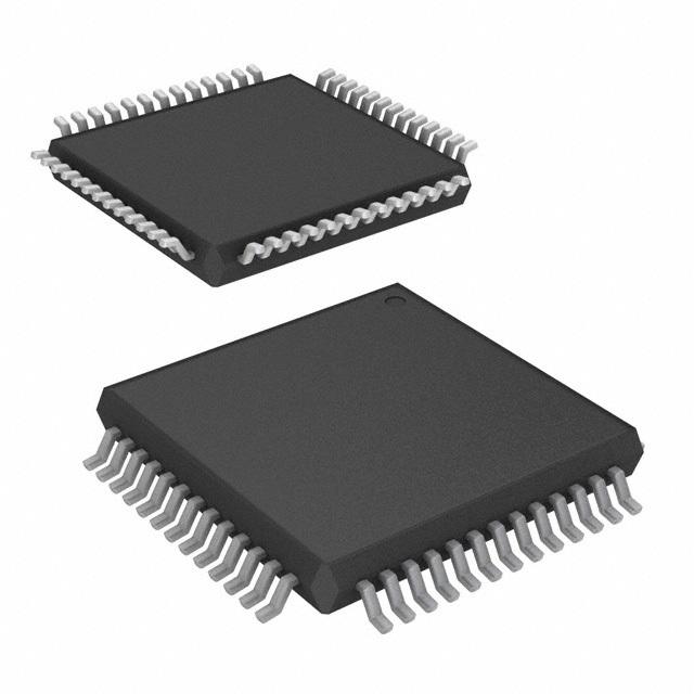
UPSD3233BV-24T6T
数据手册.pdf闪存可编程系统设备与8032微控制器内核 Flash Programmable System Device with 8032 Microcontroller Core
SUMMARY DESCRIPTION
The uPSD323x Series combines a fast 8051-based microcontroller with a flexible memory structure, programmable logic, and a rich periph eral mix including USB, to form an ideal embedded controller. At its core is an industry-standard 8032 MCU operating up to 40MHz.
A JTAG serial interface is used for In-System Programming ISP in as little as 10 seconds, perfect for manufacturing and lab development.
The USB 1.1 low-speed interface has one Control endpoint and two Interrupt endpoints suitable for HID class drivers.
The 8032 core is coupled to Programmable System Device PSD architecture to optimize the 8032 memory structure, offering two independent banks of Flash memory that can be placed at virtually any address within 8032 program or data address space, and easily paged beyond 64K bytes using on-chip programmable decode logic.
LButtonDual Flash memory banks provide a robust solution for remote product updates in the field through In-Application Programming IAP. Dual Flash banks also support EEPROM emulation, eliminat ing the need for external EEPROM chips.
FEATURES SUMMARY
■ FAST 8-BIT 8032 MCU
– 40MHz at 5.0V, 24MHz at 3.3V
– Core, 12-clocks per instruction
■ DUAL FLASH MEMORIES WITH MEMORY MANAGEMENT
– Place either memory into 8032 program address space or data address space
– READ-while-WRITE operation for In Application Programming and EEPROM emulation
– Single voltage program and erase
– 100K minimum erase cycles, 15-year retention
■ CLOCK, RESET, AND SUPPLY MANAGEMENT
– SRAM is Battery Backup capable
– Normal, Idle, and Power Down Modes
– Power-on and Low Voltage reset supervisor
– Programmable Watchdog Timer
■ PROGRAMMABLE LOGIC, GENERAL PURPOSE
– 16 macrocells
– Implements state machines, glue-logic, and so forth
■ COMMUNICATION INTERFACES
– USB v1.1, low-speed 1.5Mbps, 3 endpoints
– I2C Master/Slave bus controller
– Two UARTs with independent baud rate
– Six I/O ports with up to 46 I/O pins
– 8032 Address/Data bus available on TQFP80 package
– 5 PWM outputs, 8-bit resolution
■ JTAG IN-SYSTEM PROGRAMMING
– Program the entire device in as little as 10 seconds
■ A/D CONVERTER
– Four channels, 8-bit resolution, 10µs
■ TIMERS AND INTERRUPTS
– Three 8032 standard 16-bit timers
– 10 Interrupt sources with two external interrupt pins
■ Single Supply Voltage
– 4.5 to 5.5V
– 3.0 to 3.6V

