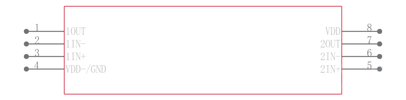
TLC252BCD
LinCMOSE双运算放大器 LinCMOSE DUAL OPERATIONAL AMPLIFIERS
The TLC252, TLC25L2, and TLC25M2 are low-cost, low-power dual operational amplifiers designed to operate with single or dual supplies. These devices utilize the Texas Instruments silicon gate LinCMOSTM process, giving them stable input offset voltages that are available in selected grades of 2, 5, or 10mV maximum, very high input impedances, and extremely low input offset and bias currents. Because the input common-mode range extends to the negative rail and the power consumption is extremely low, this series is ideally suited for battery-powered or energy-conserving applications. The series offers operation down to a 1.4-V supply, is stable at unity gain, and has excellent noise characteristics.
These devices have internal electrostatic-discharge ESD protection circuits that prevent catastrophic failures at voltages up to 2000 V as tested under MIL-STD-883C, Method 3015.1. However, care should be exercised in handling these devices as exposure to ESD may result in a degradation of the device parametric performance.
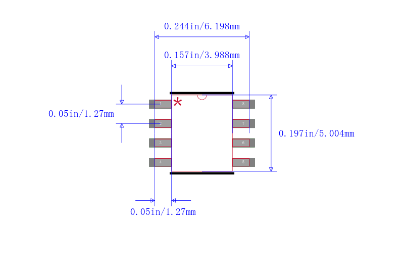
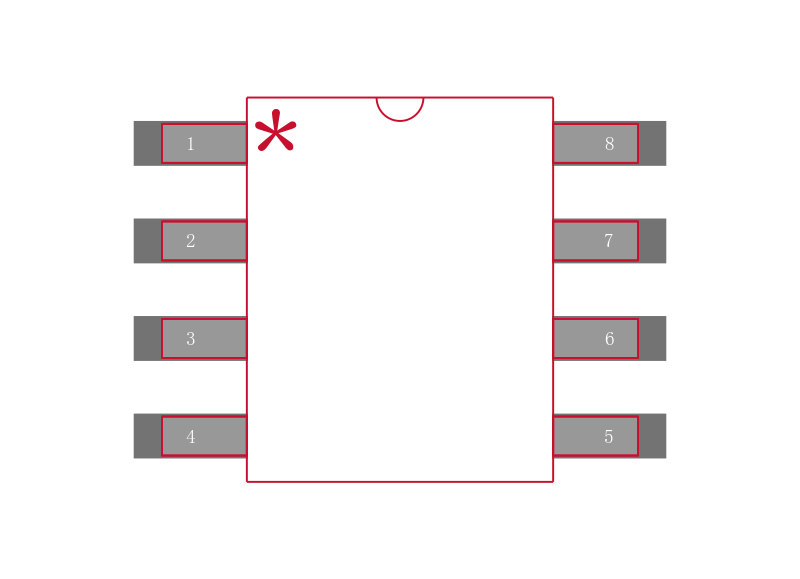
Because of the extremely high input impedance and low input bias and offset currents, applications for the TLC252/25_2 series include many areas that have previously been limited to BIFET and NFET product types. Any circuit using high-impedance elements and requiring small offset errors is a good candidate for cost-effective use of these devices. Many features associated with bipolar technology are available with LinCMOSTM operational amplifiers without the power penalties of traditional bipolar devices. General applications such as transducer interfacing, analog calculations, amplifier blocks, active filters, and signal buffering are all easily designed with the TLC252/25_2 series devices. Remote and inaccessible equipment applications are possible using their low-voltage and low-power capabilities. The TLC252/25_2 series is well suited to solve the difficult problems associated with single-battery and solar-cell-powered applications. This series includes devices that are characterized for the commercial temperature range and are available in 8-pin plastic dip and the small-outline package. The device is also available in chip form.
The TLC252/25_2 series is characterized for operation from 0°C to 70°C.