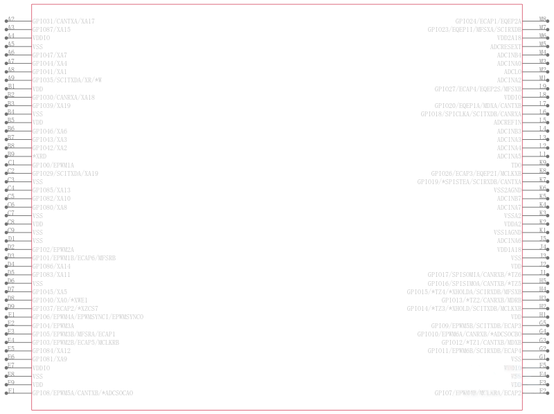
TMS320F28332ZHHA
TEXAS INSTRUMENTS TMS320F28332ZHHA 微控制器, 32位, C2000, 100 MHz, 128 KB, 52 KB, 179 引脚, BGA
Description
The TMS320F28335, TMS320F28334, TMS320F28333, TMS320F28332, TMS320F28235, TMS320F28234, and TMS320F28232 devices, members of the TMS320C28x/ Delfino™ DSC/MCU generation, are highly integrated, high-performance solutions for demanding control applications.
Features
• High-Performance Static CMOS Technology
– Up to 150 MHz 6.67-ns Cycle Time
– 1.9-V/1.8-V Core, 3.3-V I/O Design
• High-Performance 32-Bit CPU TMS320C28x
– IEEE 754 Single-Precision Floating-Point Unit FPU F2833x Only
– 16 × 16 and 32 × 32 MAC Operations
– 16 × 16 Dual MAC
– Harvard Bus Architecture
– Fast Interrupt Response and Processing
– Unified Memory Programming Model
– Code-Efficient in C/C++ and Assembly
• Six-Channel DMA Controller for ADC, McBSP, ePWM, XINTF, and SARAM
• 16-Bit or 32-Bit External Interface XINTF
– More Than 2M × 16 Address Reach
• On-Chip Memory
– F28335, F28333, F28235: 256K × 16 Flash, 34K × 16 SARAM
– F28334, F28234: 128K × 16 Flash, 34K × 16 SARAM
– F28332, F28232: 64K × 16 Flash, 26K × 16 SARAM
– 1K × 16 OTP ROM
• Boot ROM 8K × 16
– With Software Boot Modes Through SCI, SPI, CAN, I2C, McBSP, XINTF, and Parallel I/O
– Standard Math Tables
• Clock and System Control
– On-Chip Oscillator
– Watchdog Timer Module
• GPIO0 to GPIO63 Pins Can Be Connected to One of the Eight External Core Interrupts
• Peripheral Interrupt Expansion PIE Block That Supports All 58 Peripheral Interrupts
• 128-Bit Security Key/Lock
– Protects Flash/OTP/RAM Blocks
– Prevents Firmware Reverse Engineering
• Enhanced Control Peripherals
– Up to 18 PWM Outputs
– Up to 6 HRPWM Outputs With 150 ps MEP Resolution
– Up to 6 Event Capture Inputs
– Up to 2 Quadrature Encoder Interfaces
– Up to 8 32-Bit Timers 6 for eCAPs and 2 for eQEPs
– Up to 9 16-Bit Timers 6 for ePWMs and 3 XINTCTRs
• Three 32-Bit CPU Timers
• Serial Port Peripherals
– Up to 2 CAN Modules
– Up to 3 SCI UART Modules
– Up to 2 McBSP Modules Configurable as SPI
– One SPI Module
– One Inter-Integrated Circuit I2C Bus
• 12-Bit ADC, 16 Channels
– 80-ns Conversion Rate
– 2 × 8 Channel Input Multiplexer
– Two Sample-and-Hold
– Single/Simultaneous Conversions
– Internal or External Reference
• Up to 88 Individually Programmable, Multiplexed GPIO Pins With Input Filtering
• JTAG Boundary Scan Support
– IEEE Standard 1149.1-1990 Standard Test Access Port and Boundary Scan Architecture
• Advanced Emulation Features
– Analysis and Breakpoint Functions
– Real-Time Debug Using Hardware
• Development Support Includes
– ANSI C/C++ Compiler/Assembler/Linker
– Code Composer Studio™ IDE
– DSP/BIOS™ and SYS/BIOS
– Digital Motor Control and Digital Power Software Libraries
• Low-Power Modes and Power Savings
– IDLE, STANDBY, HALT Modes Supported
– Disable Individual Peripheral Clocks
• Endianness: Little Endian
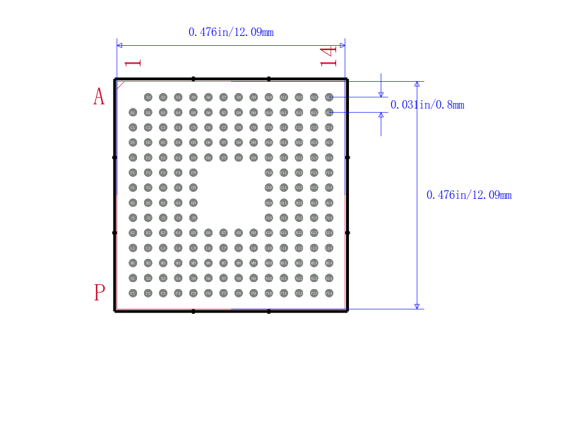
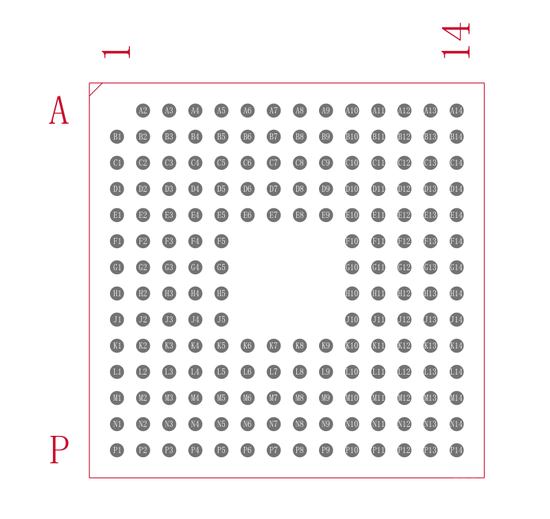
• Package Options:
– Lead-free, Green Packaging
– Plastic Ball Grid Array BGA ZJZ
– MicroStar BGA™ ZHH
– Low-Profile Quad Flatpack LQFP PGF
– Thermally Enhanced Low-Profile Quad Flatpack HLQFP PTP
• Temperature Options:
– A: –40°C to 85°C PGF, ZHH, ZJZ
– S: –40°C to 125°C PTP, ZJZ
– Q: –40°C to 125°C PTP, ZJZ
AEC Q100 Qualification for Automotive Applications
Applications
• Industrial AC Inverter Drives
• Industrial Servo Amplifiers and Controllers
• Computer Numerical Control CNC Machining
• Uninterruptible and Server Power Supplies
• Telecom Equipment Power
• Solar Inverters