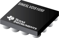
SN65LVDS1050
2.7V 双路 LVDS 发送器/接收器
The is similar to the SN65LVDS050 except that it is characterized for operation with a lower supply voltage range and packaged in the thin shrink outline package for portable battery-powered applications.
The differential line drivers and receivers use low-voltage differential signaling LVDS to achieve signaling rates as high as 400 Mbps. The drivers provide a minimum differential output voltage magnitude of 247 mV into a 100- load and receipt of 100-mV signals with up to 1 V of ground potential difference between a transmitter and receiver.
The intended application of this device and signaling technique is for point-to-point baseband data transmission over controlled impedance media of approximately 100- characteristic impedance. The transmission media may be printed-circuit board traces, backplanes, or cables. Note: The ultimate rate and distance of data transfer is dependent upon the attenuation characteristics of the media, the noise coupling to the environment and other application-specific characteristics.
The SN65LVDS1050 is characterized for operation from 40°C to 85°C.
- .
- Typically Meets or Exceeds ANSI A/EIA-644-1995 Standard
- .
- Operates From a Single 2.4-V to 3.6-V Supply
- .
- Signaling Rates up to 400 Mbit/s
- .
- Bus-Terminal ESD Exceeds 12 kV
- .
- Low-Voltage Differential Signaling With Typical Output Voltages of 285 mV and a 100 Load
- .
- Propagation Delay Times
- .
- Driver: 1.7 ns Typ
- .
- Receiver: 3.7 ns Typ
- .
- Driver: 25-mW Typical
- .
- Receiver: 60-mW Typical
- .
- Power Dissipation at 200 MHz
- .
- Driver: 25 mW Typical
- .
- Receiver: 60 mW Typical
- .
- LVTTL Input Levels Are 5 V Tolerant
- .
- Receiver Maintains High Input Impedance
- .
- Receiver Has Open-Circuit Fail Safe
- .
- Available in Thin Shink Outline Packaging With 20-mil Lead Pitch

