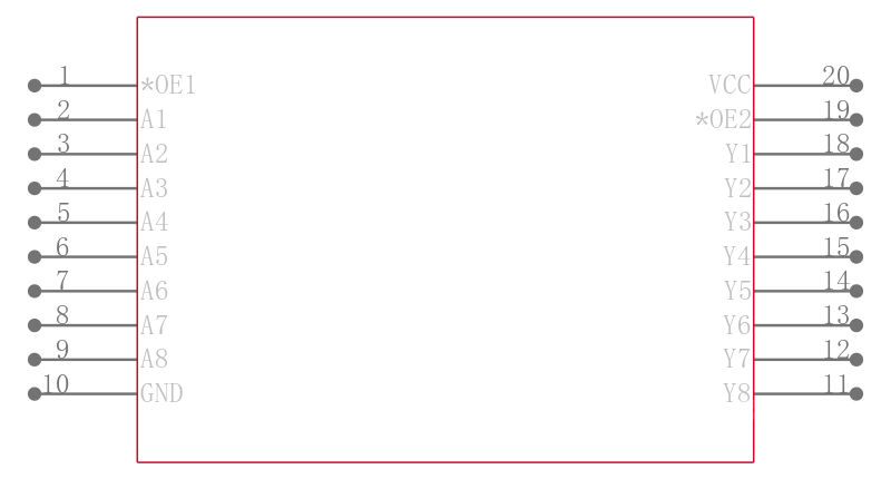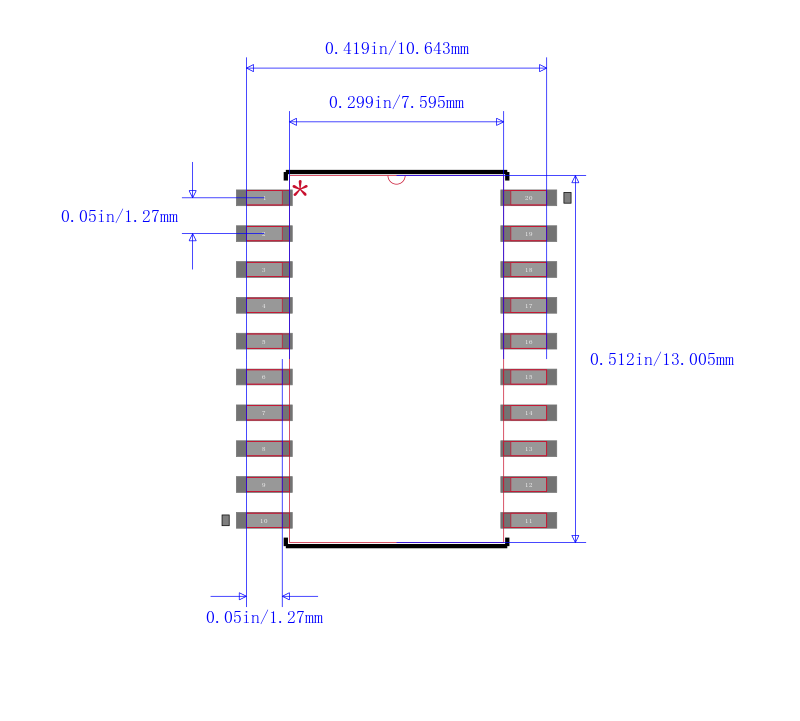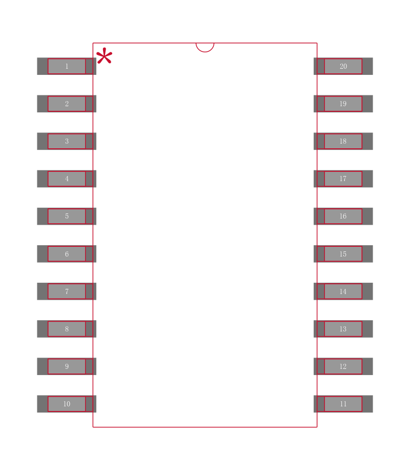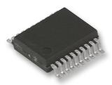
SN74LVC540ADWRE4
八路缓冲器/驱动器,具有三态输出 OCTAL BUFFERS/DRIVERS WITH 3-STATE OUTPUTS
Description
The SN54LVC540A octal buffer/driver is designed for 2.7-V to 3.6-V VCC operation, and the SN74LVC540A octal buffer/driver is designed for 1.65-V to 3.6-V VCC operation.
1 Features
1• Operate From 1.65 V to 3.6 V
• Inputs Accept Voltages to 5.5 V
• Max tpd of 5.3 ns at 3.3 V
• Typical VOLP Output Ground Bounce
< 0.8 V at VCC = 3.3 V, TA = 25°C
• Typical VOHV Output VOH Undershoot
> 2 V at VCC = 3.3 V, TA = 25°C
• Support Mixed-Mode Signal Operation on All Ports 5-V Input/Output Voltage With 3.3-V VCC
• Ioff Supports Live Insertion, Partial Power Down Mode, and Back Drive Protection
• Latch-Up Performance Exceeds 250 mA Per JESD 17
• ESD Protection Exceeds JESD 22
– 2000-V Human-Body Model A114-A
– 1000-V Charged-Device Model C101
• On Products Compliant to MIL-PRF-38535, All Parameters Are Tested Unless Otherwise Noted. On All Other Products, Production Processing Does Not Necessarily Include Testing of All Parameters.
Applications
• Handset: Smartphone
• Network Switch
• Health and Fitness; Wearables