MAX5715BAUD+
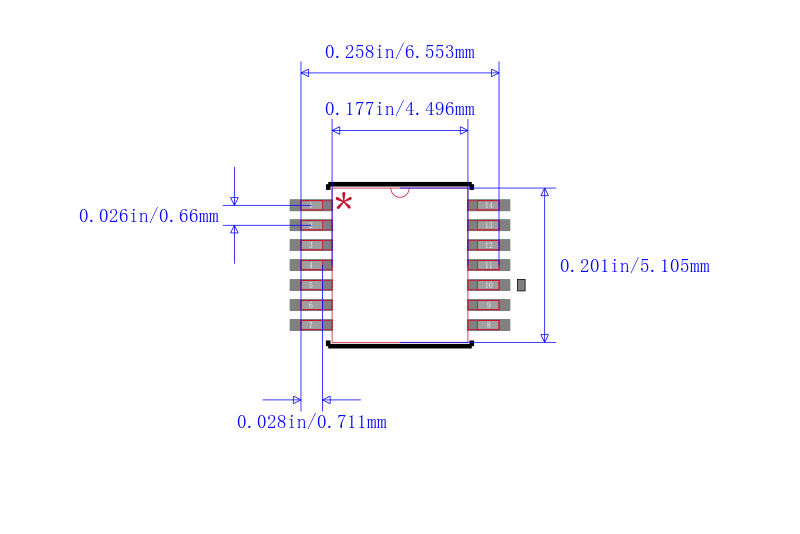
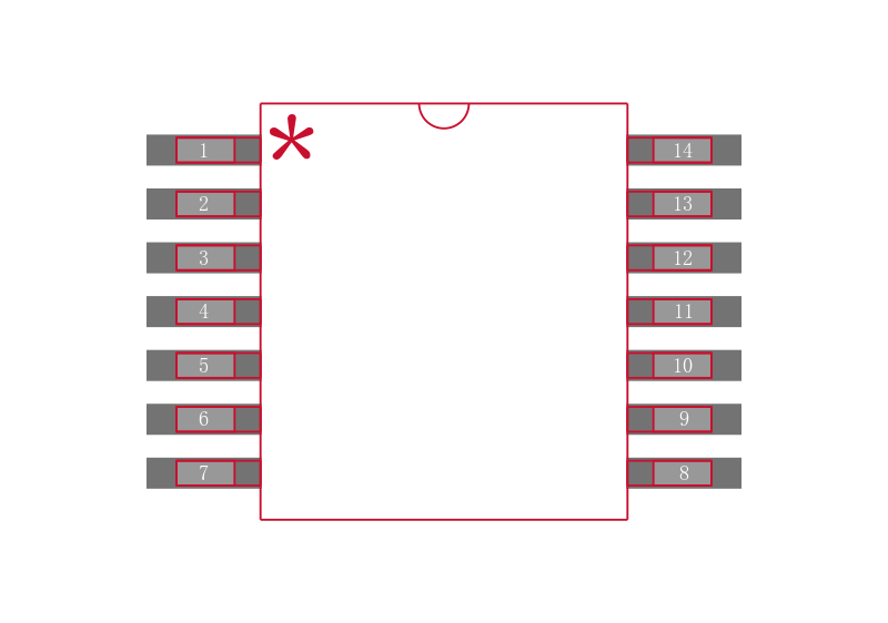
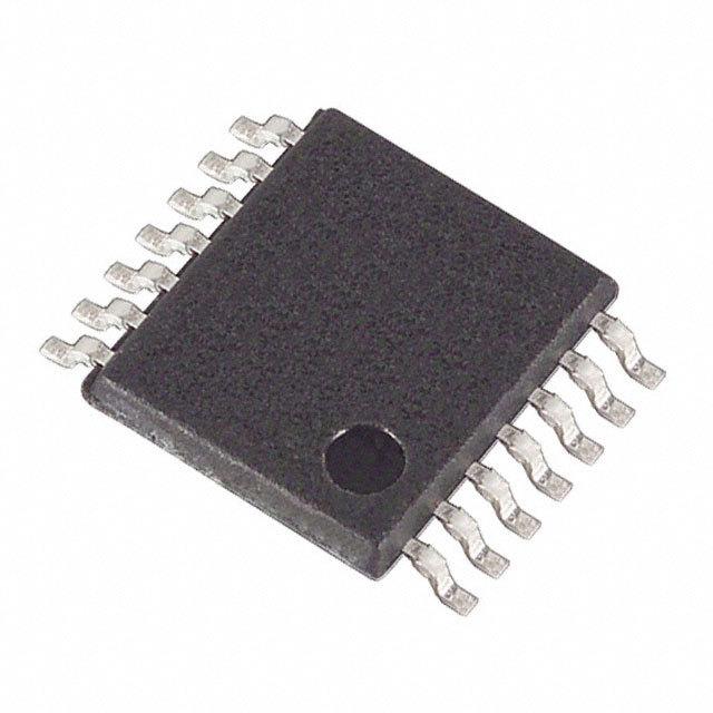
数据手册.pdfMAXIM INTEGRATED PRODUCTS MAX5715BAUD+ 数模转换器, 低功率, 12 bit, 串行, 2.7V 至 5.5V, TSSOP, 14 引脚
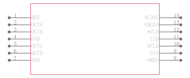
The is an ultra small, quad channel, 12bit buffered output DAC with internal reference and SPI interface in 14 pin TSSOP package. This low power, voltage output DAC includes output buffers and an internal reference that is selectable to be 2.048V, 2.500V, or 4.096V. The MAX5715B accepts a wide supply voltage range from 2.7V to 5.5V with extremely low power 3mW consumption to accommodate most low voltage applications. A precision external reference input allows rail to rail operation and presents 100Kohm load to an external reference. The device has 50MHz 3-wire SPI/QSPI/MICROWIRE/DSP compatible serial interface that also includes active-low RDY output for daisy chain applications. The DAC output is buffered and has low supply current of less than 250µA per channel and low offset error of ±0.5mV. It is used in programmable voltage and current sources, gain and offset adjustment, automatic tuning and optical control, power amplifier control and biasing data acquisition.
- .
- Power-on reset to zero scale DAC output
- .
- Operating temperature range from -40°C to 125°C
- .
- Active-low LDAC and active-low CLR pin for asynchronous control
- .
- Integral nonlinearity INL of ±0.5LSB and differential nonlinearity of ±0.2LSB
- .
- Monotonic over all operating conditions, independent mode settings for each DAC
- .
- ±0.5mV offset error, ±10µV/°C offset error drift and ±3ppm of FS/°C gain temperature coefficient
- .
- Settling time of 4.5µs and voltage output slew rate of 1V/µs
- .
- Internal reference tempco of 10ppm/°C
- .
- Zero scale error of 10mV and full scale error of ±0.5%FS
- .
- Three software selectable power down output impedances 1Kohm, 100Kohm or high impedance