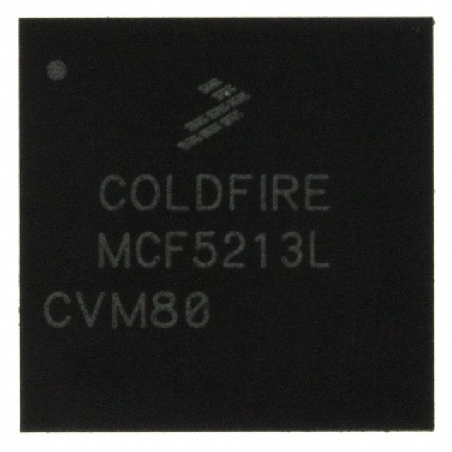
MCF51JE128CMB
数据手册.pdfMCU 32Bit MCF51JE ColdFire RISC 128KB Flash 2.5V/3.3V 81Pin MAP-BGA Tray
The MCF51JE256 series devices are members of the low-cost, low-power, high-performance ColdFire V1 family of 32-bit microcontrollers MCUs.
32-Bit ColdFire V1 Central Processor Unit CPU
• Up to 50.33 MHz ColdFire CPU above 2.4 V and 40 MHz CPU above 2.1 V and 20 MHz CPU above 1.8 V across temperature range of -40°C to 105°C.
• ColdFire Instruction Set Revision C ISA_C.
• 32-bit multiply and accumulate MAC supports signed or unsigned integer or signed fractional inputs.
On-Chip Memory
• 256 K Flash comprised of two independent 128 K flash arrays; read/program/erase over full operating voltage and temperature; allows interrupt processing while programming.
• 32 KB System Random-access memory RAM.
• Security circuitry to prevent unauthorized access to RAM and Flash contents.
Power-Saving Modes
• Two ultra-low power stop modes. Peripheral clock enable register can disable clocks to unused modules to reduce currents.
• Time of Day TOD — Ultra low-power 1/4 sec counter with up to 64 sec timeout.
• Ultra-low power external oscillator that can be used in stop modes to provide accurate clock source to the TOD. 6 µs typical wake up time from stop3 mode.
Clock Source Options
• Oscillator XOSC1 — Loop-control Pierce oscillator; 32.768 kHz crystal or ceramic resonator dedicated for TOD operation.
• Oscillator XOSC2 for high frequency crystal input for MCG reference to be used for system clock and USB operations.
• Multipurpose Clock Generator MCG — PLL and FLL; precision trimming of internal reference allows 0.2% resolution and typical +0.5% to -1% deviation over temperature and voltage; supports CPU frequencies up to 50 MHz.
System Protection
• Watchdog computer operating properly COP reset with option to run from dedicated 1 kHz internal clock source or bus clock.
• Low-voltage detection with reset or interrupt; selectable trip points; separate low voltage warning with optional interrupt; selectable trip points.
• Illegal opcode and illegal address detection with reset.
• Flash block protection for each array to prevent accidental write/erasure.
• Hardware CRC to support fast cyclic redundancy checks.
Development Support
• Integrated ColdFire DEBUG_Rev_B+ interface with single wire BDM connection supports same electrical interface used by the S08 family debug modules.
• Real-time debug with 6 hardware breakpoints 4 PC, 1 address and 1 data.
• On-chip trace buffer provides programmable start/stop recording conditions.
Input/Output
• Up to 68 GPIOs and 1 output-only pin.
• Voltage Reference output VREFO.
• Dedicated infrared output pin IRO withhigh current sink capability.
• Up to 16 KBI pins with selectable polarity.
• Up to 16 pins of rapid general purpose I/O RGPIO.
Peripherals
• USB — Dual-role USB On-The-Go OTG device, supports USB in either device, host or OTG configuration. On-chip transceiver and 3.3V regulator help save system cost, fully compliant with USB Specification 2.0. Allows control, bulk, interrupt and isochronous transfers.
• SCIx — Two serial communications interfaces with optional 13-bit break; option to connect Rx input to PRACMP output on SCI1 and SCI2; High current drive on Tx on SCI1 and SCI2; wake-up from stop3 on Rx edge.
• SPI1 — Serial peripheral interface with 32-bit FIFO buffer; 16-bit or 8-bit data transfers; full-duplex or single-wire bidirectional; double-buffered transmit and receive; master or slave mode; MSB-first or LSB-first shifting.
• SPI2 — Serial peripheral interface with full-duplex or single-wire bidirectional; Double-buffered transmit and receive; Master or Slave mode; MSB-first or LSB-first shifting.
• IIC — Up to 100 kbps with maximum bus loading; Multi-master operation; Programmable slave address; Interrupt driven byte-by-byte data transfer; supports broadcast mode and 10-bit addressing.
• CMT — Carrier Modulator timer for remote control communications. Carrier generator, modulator and driver for dedicated infrared out IRO. Can be used as an output compare timer.
• TPMx — Two 4-channel Timer/PWM Module; Selectable input capture, output compare, or buffered edge- or center-aligned PWM on each channel; external clock input/pulse accumulator.
• Mini-FlexBus — Multi-function external bus interface with user programmable chip selects and the option to multiplex address and data lines.
• PRACMP — Analog comparator with selectable interrupt; compare option to programmable internal reference voltage; operation in stop3.
• ADC12 — 12-bit Successive approximation ADC with up to12 single-ended channels; internal bandgap reference channel; operation in stop3; fully functional from 3.6V to 1.8V.
• PDB — Programmable delay block with 16-bit counter and modulus and prescale to set reference clock to bus divided by 1 to bus divided by 2048; 8 trigger outputs for ADC module provides periodic coordination of ADC sampling sequence with sequence completion interrupt; Back-to-Back mode and Timed mode.
• DAC — 12-bit resolution DAC; configurable settling time

