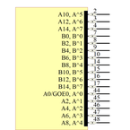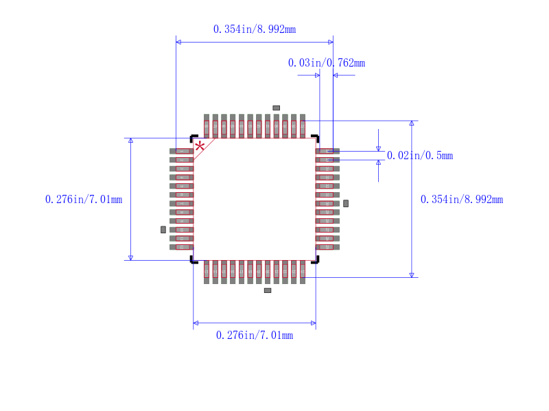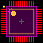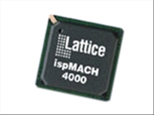
LC4064V-75TN48C
数据手册.pdfLATTICE SEMICONDUCTOR LC4064V-75TN48C 可编程逻辑芯片, CPLD, 64宏单元, 3.3V, ISPMACH, 48TQFP
The is a high performance SuperFAST CPLD consist of multiple 32-I/O, 64-macrocell. Output Routing Pools ORPs connect the GLBs to the I/O Blocks IOBs, which contain multiple I/O cells. The ispMACH 4000 family is a blend of Lattice"s two most popular architectures, the ispLSI® 2000 and ispMACH 4A. Retaining the best of both families, the ispMACH 4000 architecture focuses on significant innovations to combine the highest performance with low power in a flexible CPLD family. This family combines high speed and low power with the flexibility needed for ease of design. With its robust global routing pool and output routing pool, this family delivers excellent first-time-fit, timing predictability, routing, pin-out retention and density migration. It has enhanced system integration capabilities. Also offers enhanced I/O features such as slew rate control, PCI compatibility, bus-keeper latches, pull-up resistors, pull-down resistors, open drain outputs and hot socketing.
- .
- tPD = 2.5ns propagation delay
- .
- Up to four global clock pins with programmable clock polarity control
- .
- Up to 80 PTs per output
- .
- Enhanced macrocells with individual clock, reset, preset and clock enable controls
- .
- Up to four global OE controls
- .
- Individual local OE control per I/O pin
- .
- Excellent First-Time-Fit ™ and refit
- .
- Fast path, SpeedLocking™ Path and wide-PT path
- .
- Wide input gating 36 input logic blocks for fast counters, state machines and address decoders
- .
- Low power - 1.8V core low dynamic power
- .
- Superior solution for power sensitive consumer applications
- .
- 5V Tolerant I/O for LVCMOS 3.3, LVTTL and PCI interfaces
- .
- Hot-socketing
- .
- Open-drain capability
- .
- Input pull-up, pull-down or bus-keeper
- .
- Programmable output slew rate
- .
- 3.3V PCI compatible
- .
- IEEE 1149.1 boundary scan testable
- .
- 3.3/2.5/1.8V In-System Programmable
- .
- ISP™ Using IEEE 1532 compliant interface