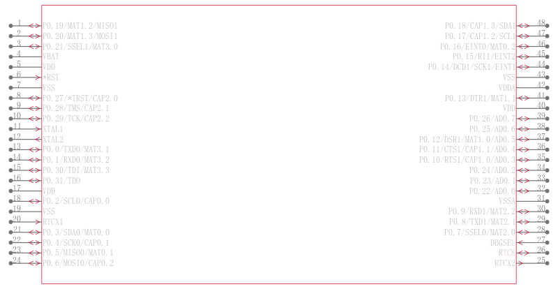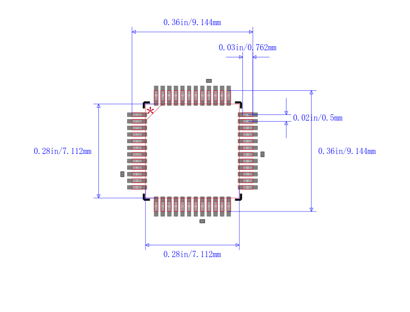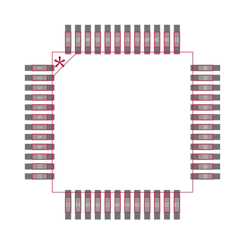
LPC2103FBD48
数据手册.pdfNXP LPC2103FBD48 微控制器, 32位, ARM7TDMI, 70 MHz, 32 KB, 8 KB, 48 引脚, LQFP
The is a 16-/32-bit Microcontroller based on ARM7TDMI-S core with real-time emulation that combines the microcontroller with 32kB of embedded high-speed flash memory. A 128-bit wide memory interface and an unique accelerator architecture enable 32-bit code execution at the maximum clock rate. For critical performance in interrupt service routines and DSP algorithms, this increases performance up to 30 % over Thumb mode. For critical code size applications, the alternative 16-bit Thumb mode reduces code by more than 30 % with minimal performance penalty. The device incorporates a blend of serial communications interfaces ranging from multiple UARTs, SPI to SSP and two I2C-buses, combined with on-chip SRAM of 8KB.
- .
- Deep power-down mode with option to retain SRAM memory and/or RTC
- .
- Three levels of flash code read protection CRP implemented
- .
- ISP/IAP via on-chip bootloader software
- .
- Single flash sector or full chip erase in 100ms and programming of 256bytes in 1ms
- .
- EmbeddedICE-RT offers real-time debugging with the on-chip RealMonitor software
- .
- The 10-bit ADC provides eight analog inputs
- .
- Two 32-bit timers/external event counters
- .
- Two 16-bit timers/external event counters
- .
- Low power real-time clock RTC
- .
- Vectored interrupt controller with configurable priorities and vector addresses
- .
- Up to thirty-two, 5V tolerant fast general purpose I/O pins
- .
- Up to 13 edge or level sensitive external interrupt pins available
- .
- 70MHz maximum CPU clock available from programmable on-chip PLL
- .
- On-chip integrated oscillator operates with an external crystal in the range from 1MHz to 25MHz
- .
- Power saving modes include Idle mode, power-down mode with RTC active and power-down mode
- .
- Individual enable/disable of peripheral functions as well as peripheral clock scaling
- .
- Processor wake-up from power-down and deep power-down mode via external interrupt or RTC