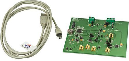
EVAL-AD5621EBZ
数据手册.pdf评估板,用于 AD5621 2.7 至 5.5V 100μA 12 位 DAC,带 SPI设计具有极低功耗和断电功能,特别适用于电池供电应用 单电源 2.7 至 5.5V 操作,最大电流消耗为 100μA 3 线串行接口,与 SPI、QSPI™、MICROWIRE™ 和 DSP 接口标准兼容 ### 数字到模拟转换器 - Analog Devices
评估板,用于 AD5621 2.7 至 5.5V 100μA 12 位 DAC,带 SPI
设计具有极低功耗和断电功能,特别适用于电池供电应用
单电源 2.7 至 5.5V 操作,最大电流消耗为 100μA
3 线串行接口,与 SPI、QSPI™、MICROWIRE™ 和 DSP 接口标准兼容
### 数字到模拟转换器 - Analog Devices
得捷:
BOARD EVALUATION FOR AD5621
欧时:
Analog Devices 模拟开发套件 EVAL-AD5621EBZ
艾睿:
AD5621AKSZ-500RL7/AD5621AKSZ-REEL7/AD5621BKSZ-500RL7/AD5621BKSZ-REEL7 DAC Evaluation Board
安富利:
The AD5601/AD5611/AD5621, members of the nanoDAC® family, are single, 8-/10-/12-bit, buffered voltage output DACs that operate from a single 2.7 V to 5.5 V supply, consuming typically 75 μA at 5 V. The parts come in tiny LFCSP and SC70 packages. Their on-chip precision output amplifier allows railto-rail output swing to be achieved. The AD5601/AD5611/ AD5621 utilize a versatile 3-wire serial interface that operates at clock rates up to 30 MHz and is compatible with SPI, QSPI™, MICROWIRE™, and DSP interface standards. The reference for the AD5601/AD5611/AD5621 is derived from the power supply inputs and, therefore, gives the widest dynamic output range. The parts incorporate a power-on reset circuit, which ensures that the DAC output powers up to 0 V and remains there until a valid write to the device takes place. The AD5601/AD5611/AD5621 contain a power-down feature that reduces current consumption to typically 0.2 μA at 3 V. They also provide software-selectable output loads while in
Chip1Stop:
2.7 V TO 5.5 V 100 UA 8-/10-/12-BIT NANODAC SPI INTERFACE IN SC70 PACKAGE
Verical:
AD5621AKSZ-500RL7/AD5621AKSZ-REEL7/AD5621BKSZ-500RL7/AD5621BKSZ-REEL7 DAC Evaluation Board
Newark:
# ANALOG DEVICES EVAL-AD5621EBZ Evaluation Board, Data Converter, DAC, 12-Bits, 1.7MSPS, AD5621, Nano Size