ADN4664BRZ-REEL7
数据手册.pdfLVDS Receiver 400Mbps 8Pin SOIC N T/R
Product Details
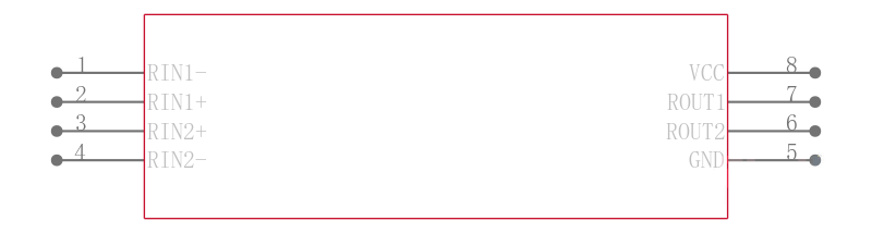
The ADN4664 is a dual, CMOS, low voltage differential signaling LVDS line receiver offering data rates of over 400 Mbps 200 MHz and ultralow power consumption. It features a flow-through pinout for easy PCB layout and separation of input and output signals. The device accepts low voltage 310 mV typical differential input signals and converts them to a single-ended 3 V TTL/CMOS logic level.
The ADN4664 and its companion driver, the ADN4663, offer a new solution to high speed, point-to-point data transmission, and a low power alternative to emitter-coupled logic ECL or positive emitter-coupled logic PECL.
** Applications**
* Point-to-point data transmission
* Multidrop buses
* Clock distribution networks
* Backplane receivers
### Features and Benefits
- .
- ±15 kV ESD protection on output pins
- .
- 400 Mbps 200 MHz switching rates
- .
- Flow-through pinout simplifies PCB layout
- .
- 100 ps channel-to-channel skew typical
- .
- 2.5 ns maximum propagation delay
- .
- 3.3 V power supply
|
- .
- High impedance outputs on power-down
- .
- Low power design: typically 3 mW quiescent
- .
- Interoperable with existing 5 V LVDS drivers
- .
- Accepts small swing 310 mV typical differential signal levels
- .
- Supports open, short, and terminated input fail-safe
- .
- 0 V to −100 mV threshold region
---|---