AD8079AR
数据手册.pdf双260 MHz增益= 2.0 & 2.2缓冲区 Dual 260 MHz Gain = +2.0 & +2.2 Buffer
Product Details
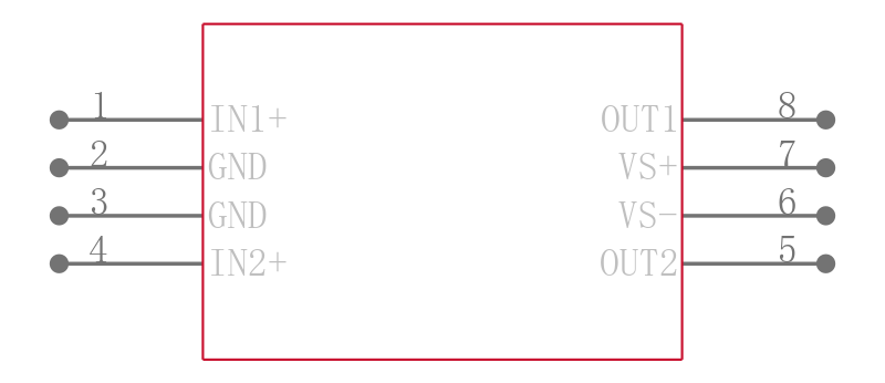
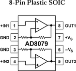
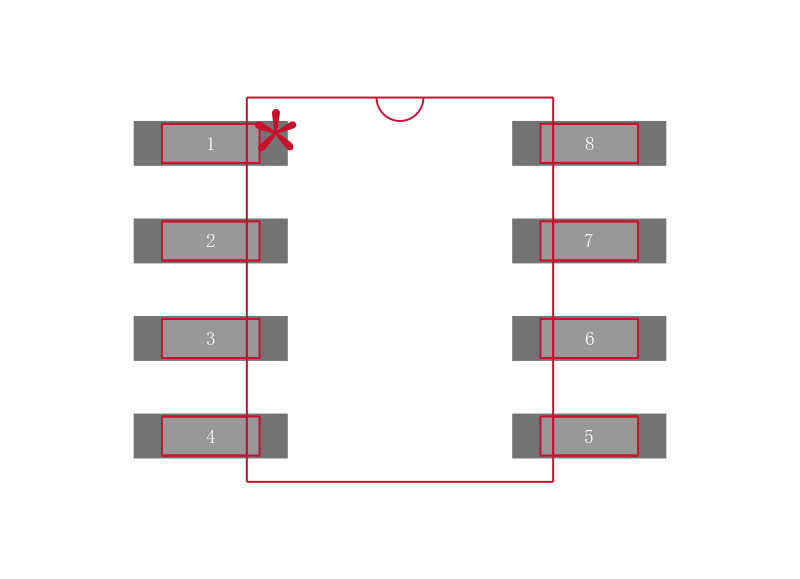
The AD8079 is a dual, low power, high speed buffer designed to operate on ±5 V supplies. The AD8079"s pinout offers excellent input and output isolation compared to the traditional dual amplifier pin configuration. With two ac ground pins separating both the inputs and outputs, the AD8079 achieves very low crosstalk of less than -70 dB at 5 MHz.
Additionally, the AD8079 contains gain setting resistors factory set at G = +2.0 A grade or Gain = +2.2 B grade allowing circuit configurations with minimal external components. The B grade gain of +2.2 compensates for gain loss through a system by providing a single-point trim. Using active laser trimming of these resistors, the AD8079 guarantees tight control of gain and channel-channel gain matching. With its performance and figuration, the AD8079 is well suited for driving differential cables and transformers. Its low distortion and fast settling are ideal for buffering high speed dual or differential A-to-D converters.
The AD8079 features a unique transimpedance linearization circuitry. This allows it to drive video loads with excellent differential gain and phase performance of 0.01% and 0.02° on only 50 mW of power per amplifier. It features gain flatness of 0.1 dB to 50 MHz. This makes the AD8079 ideal for professional video electronics such as cameras and video switchers.
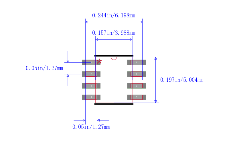
The AD8079 offers low power of 5 mA/amplifier VS = ±5 V and can run on a single +12 V power supply while delivering over 70 mA of load current. All of this is offered in a small 8-pin SOIC package. These features make this amplifier ideal for portable and battery powered applications where size and power are critical.
The outstanding bandwidth of 260 MHz along with 800 V/µs of slew rate make the AD8079 useful in many general purpose high speed applications where dual power supplies of ±3 V to ±6 V are required.
The AD8079 is available in the industrial temperature range of -40°C to +85°C.
### Features and Benefits
- .
- Factory Set Gain
Gain of 2.2 Compensates for System Gain Loss
Minimizes External Components
Tight Control of Gain and Gain Matching 0.1%
- .
- Optimum Dual Pinout
Simplifies PCB Layout
Low Crosstalk of -70dB @ 5MHz
- .
- Excellent Video Specifications RL=150 Ω
Gain Flatness 0.1dB to 50MHz
0.01% Differential Gain Error
0.02° Differential Phase Error
- .
- Low Power of 50 mW/Amplifier 5mA
- .
- High Speed and Fast Settling
260MHz, -3dB Bandwidth
750 V/µs Slew Rate 2 V Step, 800 V/µs 4 V Step
40 ns Settling Time to 0.1% 2V Step
- .
- Low Distortion of -65dBc THD, fc=5MHz
- .
- High Output Drive of Over 70mA