AD620BRZ-R7
数据手册.pdf低成本低功耗仪表放大器 Low Cost Low Power Instrumentation Amplifier
Product Details
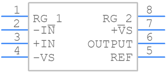
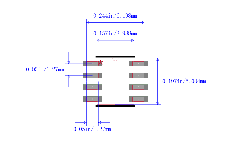
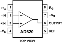
The AD620 is a low cost, high accuracy instrumentation amplifier that requires only one external resistor to set gains of 1 to 10,000. Furthermore, the AD620 features 8-lead SOIC and DIP packaging that is smaller than discrete designs and offers lower power only 1.3 mA max supply current, making it a good fit for battery powered, portable or remote applications.
The AD620, with its high accuracy of 40 ppm maximum nonlinearity, low offset voltage of 50 µV max, and offset drift of 0.6 µV/°C max, is ideal for use in precision data acquisition systems, such as weigh scales and transducer interfaces. Furthermore, the low noise, low input bias current, and low power of the AD620 make it well suited for medical applications such as ECG and noninvasive blood pressure monitors.
The low input bias current of 1.0 nA max is made possible with the use of Superϐeta processing in the input stage. The AD620 works well as a preamplifier due to its low input voltage noise of 9 nV/√Hz at 1 kHz, 0.28 μV p-p in the 0.1 Hz to 10 Hz band, and 0.1 pA/√Hz input current noise. Also, the AD620 is well suited for multiplexed applications with its settling time of 15 μs to 0.01%, and its cost is low enough to enable designs with one in-amp per channel.
### Features and Benefits
- .
- EASY TO USE
Gain Set with One External Resistor
Gain Range 1 to 10,000
Wide Power Supply Range ±2.3 V to ±18 V
Higher Performance than Three
Op Amp IA Designs
Available in 8-Lead DIP and SOIC Packaging
Low Power, 1.3 mA max Supply
- .
- LOW NOISE
9 nV/√Hz, @ 1 kHz, Input Voltage Noise
0.28 µV p-p Noise 0.1 Hz to 10 Hz
- .
- EXCELLENT DC PERFORMANCE B GRADE
50 µV max, Input Offset Voltage
0.6 µV/°C max, Input Offset Drift
1.0 nA max, Input Bias Current
100 dB min Common-Mode
Rejection Ratio G = 10
- .
- EXCELLENT AC SPECIFICATIONS
120 kHz Bandwidth G = 100
15 µs Settling Time to 0.01%