AD8666WARZ-R7
数据手册.pdf16 V , 4 MHz的RR0放大器 16 V, 4 MHz RR0 Amplifiers
Product Details
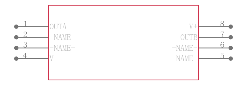
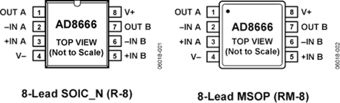
The AD866x family are single supply, rail-to-rail output amplifiers with low noise performance featuring an extended operating range with supply voltages up to 16 V. They also feature low input bias currents, wide signal bandwidth, and low input voltage and current noise. For lower offset voltage, choose the AD8661/AD8662/AD8664 family.
The combination of low offsets, very low input bias currents, and wide supply range make these amplifiers useful in a wide variety of cost sensitive applications normally associated with much higher priced JFET amplifiers. Systems using high impedance sensors, such as photo diodes, benefit from the combination of low input bias current, low noise, and low offset and bandwidth. The wide operating voltage range matches high performance ADCs and DACs. Audio applications and medical monitoring equipment can take advantage of the high input impedance, low voltage and current noise, wide bandwidth, and the lack of popcorn noise found in many other low input bias current amplifiers.
The AD866x family is specified over the extended industrial temperature range −40° to +125°C. See the Ordering Guide for automotive models.
**Applications **
* Sensor amplification
* Reference buffers
* Medical equipment
* Physiological measurements
* Signal filters and conditioning
* Consumer audio
* Photodiode amplification
* ADC driver
* Level shifting circuits
### Features and Benefits
- .
- Offset Voltage: 2.5 mV Max
- .
- Low Input Bias Current: 1 pA Max
- .
- Single-supply Operation: 5 V to 16 V
- .
- Dual-supply Operation: ±2.5 V to ±8 V
- .
- Low Noise: 8 nV/√Hz @ 10 kHz
- .
- Wide Bandwidth: 4 MHz
- .
- Rail-to-rail Output
- .
- Unity Gain Stable
- .
- Lead-free Packaging
- .
- Qualified for automotive applications.