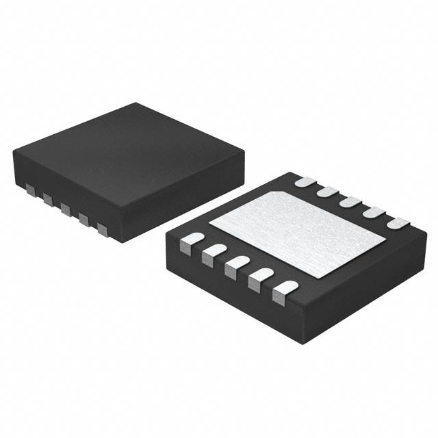
ADP2504ACPZ-3.5-R7
数据手册.pdf升降压型 Vin=2.3V~5.5V Vout=3.5V 1A
Product Details
The ADP2503/ADP2504 are high efficiency, low quiescent current step-up/step-down dc-to-dc converters that can operate at input voltages greater than, less than, or equal to the regulated output voltage. The power switches and synchronous rectifiers are internal to minimize external part count. At high load currents, the ADP2503/ADP2504 use a current-mode, fixed frequency pulse-width modulation PWM control scheme for optimal stability and transient response. To ensure the longest battery life in portable applications, the ADP2503/ADP2504 have an optional power save mode that reduces the switching frequency under light load conditions. For wireless and other low noise applications where variable frequency power save mode may cause interference, the logic control input sync forces fixed frequency PWM operation under all load conditions.
The ADP2503/ADP2504 can run from input voltages between 2.3 V and 5.5 V, allowing single lithium or lithium polymer cell, multiple alkaline or NiMH cells, PCMCIA, USB, and other standard power sources. The ADP2503/ADP2504 have fixed output options, or using the adjustable model, the output voltage can be programmed through an external resistor divider. Compensation is internal to minimize the number of external components.
During logic-controlled shutdown, the input is disconnected from the output and draws less than 1 μA from the input source. Operating as boost converters, the ADP2503/ADP2504 feature a true load disconnect function that isolates the load from the power source. Other key features include undervoltage lockout to prevent deep battery discharge, and soft start to prevent input current overshoot at startup.
**Applications**
* Wireless handsets
* Digital cameras/portable audio players
* Miniature hard disk power supplies
* USB powered devices
Data Sheet, Rev. A, 08/09
### Features and Benefits
- .
- 1 mm height profile
- .
- Compact PCB footprint
- .
- Seamless transition between modes
- .
- 38 μA typical quiescent current
- .
- 2.5 MHz operation enables 1.5 μH inductor
- .
- Input voltage: 2.3 V to 5.5 V
- .
- Fixed output voltage: 2.8 V to 5.0 V
- .
- See data sheet for additional features