AD5371BSTZ
数据手册.pdfANALOG DEVICES AD5371BSTZ 数模转换器, 14 bit, 540 kSPS, 串行, 2.5V 至 5.5V, LQFP, 80 引脚
Product Details
The AD5371- .
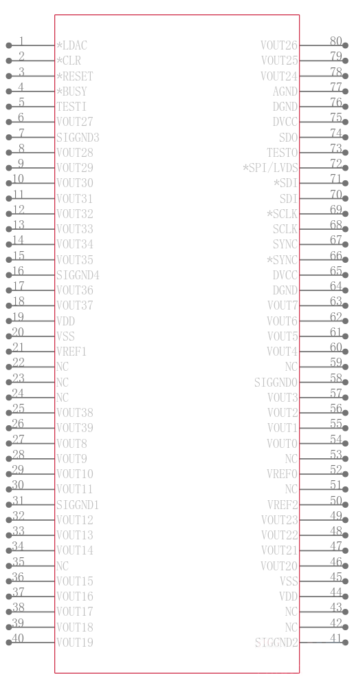
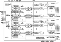
- contains 40 14-bit DACs in a single 80-lead LQFP or 100-ball CSP_BGA. The device provides buffered voltage outputs with a span of 4× the reference voltage. The gain and offset of each DAC can be independently trimmed to remove errors. For even greater flexibility, the device is divided into five groups of eight DACs. Three offset DACs allow the output range of the groups to be adjusted. Group 0 can be adjusted by Offset DAC 0, Group 1 can be adjusted by Offset DAC 1, and Group 2 to Group 4 can be adjusted by Offset DAC 2.
The AD5371 offers guaranteed operation over a wide supply range, with VSS from −16.5 V to −4.5 V and VDD from 9 V to 16.5 V. The output amplifier headroom requirement is 1.4 V operating with a load current of 1 mA.
The AD5371 has a high speed serial interface that is compatible with SPI, QSPI™, MICROWIRE™, and DSP interface standards and can handle clock speeds of up to 50 MHz. It also has a 100 MHz low voltage differential signaling LVDS serial interface.
The DAC registers are updated on reception of new data. All the outputs can be updated simultaneously by taking the LDAC input low. Each channel has a programmable gain and an offset adjust register to allow removal of gain and offset errors.
Each DAC output is gained and buffered on chip with respect to an external SIGGNDx input. The DAC outputs can also be switched to SIGGNDx via the CLR pin.
**Applications**
- .
- Level setting in automatic test equipment ATE
- .
- Variable optical attenuators VOA
- .
- Optical switches
- .
- Industrial control systems
- .
- Instrumentation
*Protected by U.S. Patent No. 5,969,657; other patents pending.
### Features and Benefits
- .
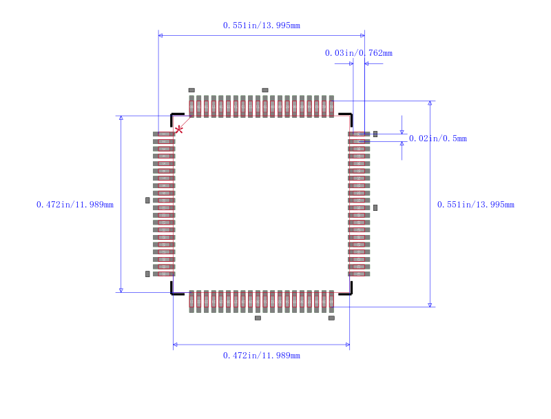
- 40-channel DAC in 80-lead LQFP and 100-ball CSP_BGA
- .
- Guaranteed monotonic to 14 bits
- .
- Maximum output voltage span of
4 × VREF
20 V
- .
- Nominal output voltage span of −4 V to +8 V
- .
- System calibration function allowing user-programmable offset and gain
- .
- Clear function to user-defined SIGGNDx
- .
- Multiple, independent output spans available
- .
- See Data Sheet for Additional Information