AD9152BCPZ
数据手册.pdfANALOG DEVICES AD9152BCPZ 数模转换器, 低功率, 16 bit, 2.25 GSPS, 串行, 3.13V 至 3.47V, LFCSP, 56 引脚
Product Details
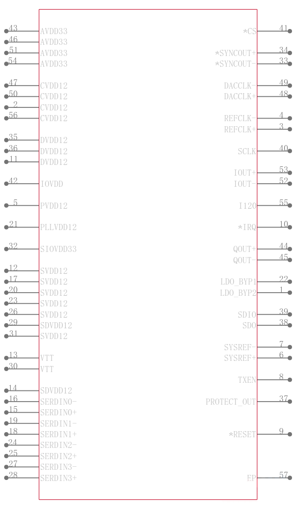
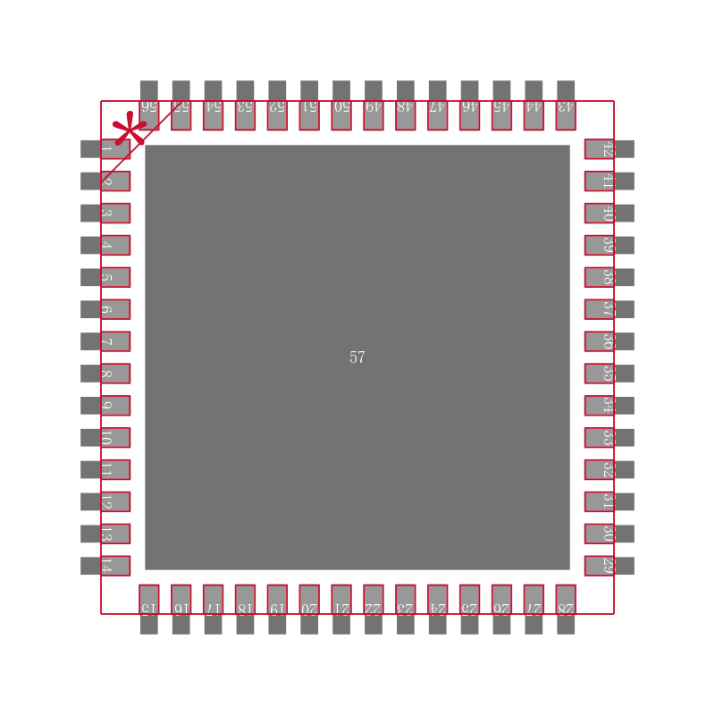
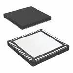
The AD9152 is a dual, 16-bit, high dynamic range digital-to-analog converter DAC that provides a maximum sample rate of 2.25 GSPS, permitting a multicarrier generation up to the Nyquist frequency. The DAC outputs are optimized to interface seamlessly with the ADRF6720 analog quadrature modulator AQM from Analog Devices, Inc. An optional 3-wire or 4-wire serial port interface SPI provides for programming/readback of many internal parameters. The full-scale output current can be programmed over a range of 4 mA to 20 mA. The AD9152 is available in a 56-lead LFCSP. The AD9152 is a member of the TxDAC+® family.
**Product Highlights**
1. Ultrawide signal bandwidth enables emerging wideband and multiband wireless applications.
2. Advanced low spurious and distortion design techniques provide high quality synthesis of wideband signals from baseband to high intermediate frequencies.
3. JESD204B Subclass 1 support simplifies multichip synchronization in software and hardware design.
4. Fewer pins for data interface width with the serializer/deserializer SERDES JESD204B four-lane interface.
5. Programmable transmit enable function allows easy design balance between power consumption and wake-up time.
6. Small package size with an 8 mm × 8 mm footprint.
**Applications**
- .
- Wireless communications
- .
- Multicarrier LTE and GSM base stations
- .
- Wideband repeaters
- .
- Software defined radios
- .
- Wideband communications
- .
- Point to point microwave radios
- .
- LMDS/MMDS
- .
- Transmit diversity, multiple input/multiple output MIMO
- .
- Instrumentation
- .
- Automated test equipment
### Features and Benefits
- .
- Supports input data rates up to 1.125 GSPS
- .
- Proprietary low spurious and distortion design
- .
- Single carrier LTE 20 MHz bandwidth BW, ACLR = 77 dBc
at 180 MHz IF
- .
- SFDR = 72 dBc at 150 MHz IF, −6 dBFS
- .
- Flexible 4-lane JESD204B interface
- .
- Multiple chip synchronization
- .
- Fixed latency
- .
- Data generator latency compensation
- .
- Selectable 1×, 2×, 4×, and 8× interpolation filter
- .
- Low power architecture
- .
- Input signal power detection
- .
- Emergency stop for downstream analog circuitry protection
- .
- Transmit enable function allows extra power saving
- .
- High performance, low noise, phase-locked loop PLL clock multiplier
- .
- Digital inverse sinc filter and programmable finite impulse response FIR filter
- .
- Low power: 1223 mW at 1.5 GSPS, 1406 mW at 2.0 GSPS, full operating conditions
- .
- 56-lead LFCSP with exposed pad