ADV7125JSTZ240
数据手册.pdfANALOG DEVICES ADV7125JSTZ240 数模转换器, 8 bit, 240 MSPS, 并行, 3V 至 3.6V, 4.75V 至 5.25V, LQFP, 48 引脚
Product Details
The ADV7125 ADV® is a triple high speed, digital-to-analog converter DAC on a single monolithic chip. It consists of three high speed, 8-bit video DACs with complementary outputs, a standard TTL input interface, and a high impedance, analog output current source.
The ADV7125 has three separate 8-bit-wide input ports. A single +5 V/+3.3 V power supply and clock are all that are required to make the device functional. The ADV7125 has additional video control signals, composite SYNC and BLANK as well as a power save mode.
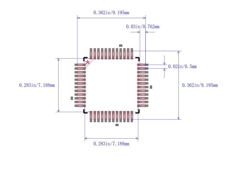
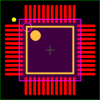
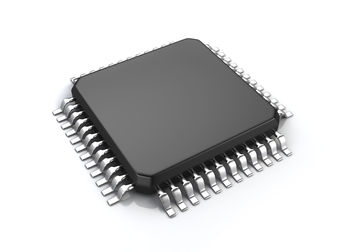
The ADV7125 is fabricated in a 5 V CMOS process. Its monolithic CMOS construction ensures greater functionality with lower power dissipation. The ADV7125 is available in 48- lead LQFP and 48-lead LFCSP packages.
Product Highlights
1. 330 MSPS 3.3 V only throughput.
2. Guaranteed monotonic to eight bits.
3. Compatible with a wide variety of high resolution color graphics systems, including RS-343A and RS-170.
Applications
- .
- Digital video systems
- .
- High resolution color graphics
- .
- Digital radio modulation
- .
- Image processing
- .
- Instrumentation
- .
- Video signal reconstruction
- .
- Automotive infotainment units
### Features and Benefits
- .
- 330 MSPS throughput rate
- .
- Triple 8-bit DACs
- .
- RS-343A-/RS-170-compatible output
- .
- Complementary outputs
- .
- DAC output current range: 2.0 mA to 26.5 mA
- .
- TTL-compatible inputs
- .
- Internal reference 1.235 V
- .
- Single-supply +5 V/+3.3 V operation
- .
- 48-lead LQFP and LFCSP
- .
- Low power dissipation 30 mW minimum at 3 V
- .
- Low power standby mode 6 mW typical at 3 V
- .
- Industrial temperature range −40°C to +85°C
- .
- RoHS compliant packages
- .
- Qualified for automotive applications