ADV7123KSTZ140-RL
数据手册.pdfADV7123KSTZ140-RL 编带
Product Details
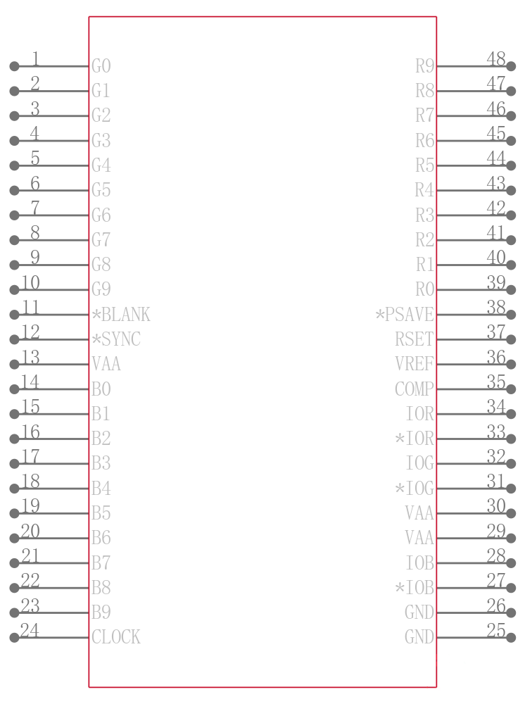
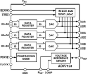
The ADV7123 ADV® is a triple high speed, digital-to-analog converter on a single monolithic chip. It consists of three high speed, 10-bit, video DACs with complementary outputs, a standard TTL input interface, and a high impedance, analog output current source.
The ADV7123 has three separate 10-bit-wide input ports. A single 5 V/3.3 V power supply and clock are all that are required to make the part functional. The ADV7123 has additional video control signals, composite SYNC and BLANK.
The ADV7123 also has a power save mode.
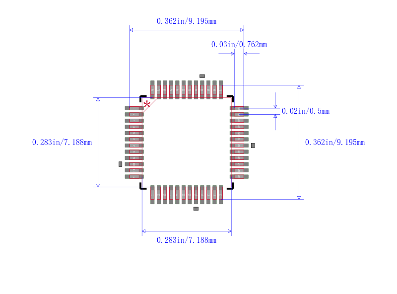
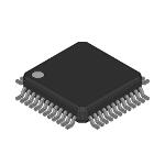
The ADV7123 is fabricated in a 5 V CMOS process. Its monolithic CMOS construction ensures greater functionality with lower power dissipation. The ADV7123 is available in a 48-lead LQFP package.
**Product Highlights**
1. 330 MSPS throughput.
2. Guaranteed monotonic to 10 bits.
3. Compatible with a wide variety of high resolution color graphics systems, including RS-343A and RS-170.
**Applications**
- .
- Digital video systems 1600 × 1200 at 100 Hz
- .
- High resolution color graphics
- .
- Digital radio modulation
- .
- Image processing
- .
- Instrumentation
- .
- Video signal reconstruction
### Features and Benefits
- .
- 330 MSPS throughput rate
- .
- Triple 10-bit digital-to-analog converters DACs
- .
- SFDR
- .
- −70 dB at fCLK = 50 MHz; fOUT = 1 MHz
- .
- −53 dB at fCLK = 140 MHz; fOUT = 40 MHz
- .
- RS-343A-/RS-170-compatible output
- .
- Complementary outputs
- .
- DAC output current range: 2.0 mA to 26.5 mA
- .
- TTL-compatible inputs
- .
- Internal reference 1.235 V
- .
- Single-supply 5 V/3.3 V operation
- .
- 48-lead LQFP package
- .
- See data sheet for additional features
ADV7123-EP supports defense and aerospace applications AQEC standard
- .
- Download ADV7123-EP data sheet pdf
- .
- Military temperature range: −55°C to +105°C
- .
- Controlled manufacturing baseline
- .
- One assembly/test site
- .
- One fabrication site
- .
- Enhanced product change notification
- .
- Qualification data available on request
- .
- V62/12637 DSCC Drawing Number