AD7707BRUZ-REEL7
数据手册.pdfAnalog to Digital Converters - ADC 3V/5V +/-10V Input Range 1mW 3CH 16B
Product Details
The AD7707 is a complete analog front end for low frequency measurement applications. This 3-channel device can accept either low level input signals directly from a transducer or high level ±10 V signals and produce a serial digital output. It employs a Σ-Δ conversion technique to realize up to 16 bits of no missing codes performance. The selected input signal is applied to a proprietary programmable gain front end based around an analog modulator. The modulator output is processed by an on-chip digital filter. The first notch of this digital filter can be programmed via an on-chip control register allowing adjustment of the filter cutoff and output update rate.
The AD7707 operates from a single 2.7 V to 3.3 V or 4.75 V to 5.25 V supply. The AD7707 features two low level pseudo differential analog input channels, one high level input channel and a differential reference input. Input signal ranges of 0 mV to 20 mV through 0 V to 2.5 V can be accommodated on both low level input channels when operating with a VDD of 5 V and a reference of 2.5 V. They can also handle bipolar input signal ranges of ±20 mV through ±2.5 V, which are referenced to the LCOM input. The AD7707, with a 3 V supply and a 1.225 V reference, can handle unipolar input signal ranges of 0 mV to 10 mV through 0 V to 1.225 V. Its bipolar input signal ranges are ±10 mV through ±1.225 V. The high level input channel can accept input signal ranges of ±10 V, ±5 V, 0 V to 10 V and 0 V to 5 V. The AD7707 thus performs all signal conditioning and conversion for a 3-channel system.
The AD7707 is ideal for use in smart, microcontroller or DSP- based systems. It features a serial interface that can be configured for 3-wire operation. Gain settings, signal polarity and update rate selection can be configured in software using the input serial port. The part contains self-calibration and system calibration options to eliminate gain and offset errors on the part itself or in the system.
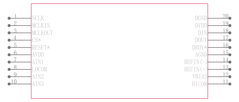
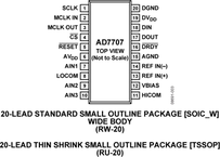
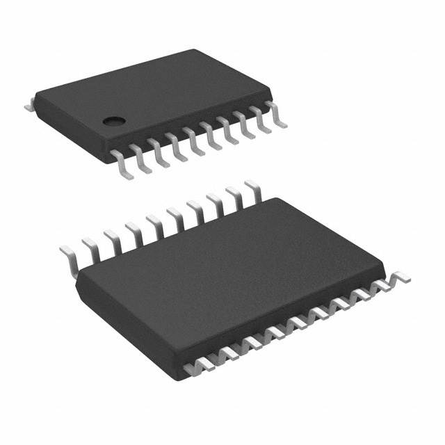
CMOS construction ensures very low power dissipation, and the power-down mode reduces the standby power consumption to 20 μW typical. This part is available in a 20-lead wide body 0.3 inch small outline SOIC package and a low profile 20-lead TSSOP.
**Product Highlights**
1. The AD7707 consumes less than 1 mW at 3 V supplies and 1 MHz master clock, making it ideal for use in low power systems. Standby current is less than 8 μA.
2. On-chip thin-film resistors allow ±10 V, ±5 V, 0 V to 10 V, and 0 V to 5 V high level input signals to be directly accom- modated on the analog inputs without requiring split supplies or charge-pumps.
3. The low level input channels allow the AD7707 to accept input signals directly from a strain gage or transducer removing a considerable amount of signal conditioning.
4. The part features excellent static performance specifications with 16 bits, no missing codes, ±0.003% accuracy, and low rms noise. Endpoint errors and the effects of temperature drift are eliminated by on-chip calibration options, which remove zero-scale and full-scale errors.
### Features and Benefits
- .
- Charge balancing ADC
16 bits no missing codes
0.003% nonlinearity
- .
- High level ±10 V and low level ±10 mV input channels
- .
- True bipolar ±100 mV capability on low level input
Channels without requiring charge pumps
- .
- Programmable gain front end
- .
- Gains from 1 to 128
- .
- 3-wire serial interface
SPI®, QSPI™, MICROWIRE™ and DSP Compatible
Schmitt trigger input on SCLK
- .
- Ability to buffer the analog input
- .
- 2.7 V to 3.3 V or 4.75 V to 5.25 V operation
- .
- Power dissipation 1 mW @ 3 V
- .
- Standby current 8 µA max
- .
- 20-Lead SOIC and TSSOP Packages