AD9704BCPZ
数据手册.pdf8位/ 10位/ 12位/ 14位, 175 MSPS TxDAC系列D / A转换器 8-/10-/12-/14-Bit, 175 MSPS TxDAC D/A Converters
Product Details
The AD9704/AD9705/AD9706/AD9707 are the fourth-generation family in the TxDAC series of high performance, CMOS digital-to-analog converters DACs. This pin-compatible, 8-/10-/12-/14-bit resolution family is optimized for low power operation, while maintaining excellent dynamic performance. The AD9704/AD9705/AD9706/AD9707 family is pin-compatible with the AD9748/AD9740/AD9742/AD9744 family of TxDAC converters and is specifically optimized for the transmit signal path of communication systems. All of the devices share the same interface, LFCSP_VQ package, and pinout, providing an upward or downward component selection path based on performance, resolution, and cost. The AD9704/AD9705/AD9706/AD9707 offers exceptional ac and dc performance, while supporting update rates up to 175 MSPS.
The flexible power supply operating range of 1.7 V to 3.6 V and low power dissipation of the AD9704/AD9705/AD9706/AD9707 parts make them well suited for portable and low power applications.
Power dissipation of the AD9704/AD9705/AD9706/AD9707 can be reduced to 15 mW, with a small trade-off in performance, by lowering the full-scale current output. In addition, a power-down mode reduces the standby power dissipation to approximately 2.2 mW.
The AD9704/AD9705/AD9706/AD9707 has an optional serial peripheral interface SPI® that provides a higher level of programmability to enhance performance of the DAC. An adjustable output, common-mode feature allows for easy interfacing to other components that require common modes from 0 V to 1.2 V.
Edge-triggered input latches and a 1.0 V temperature-compensated band gap reference have been integrated to provide a complete, monolithic DAC solution. The digital inputs support 1.8 V and 3.3 V CMOS logic families.
**Product Highlights**
1. Pin Compatible. The AD9704/AD9705/AD9706/AD9707 line of TxDAC® converters is pin-compatible with theAD9748/AD9740/AD9742/AD9744 TxDAC line LFCSP_VQ package.
2. Low Power. Complete CMOS DAC operates on a single supply of 3.6 V down to 1.7 V, consuming 50 mW 3.3 Vand 12 mW 1.8 V. The DAC full-scale current can be reduced for lower power operation. Sleep and power-down modes are provided for low power idle periods.
3. Self-Calibration. Self-calibration enables true 14-bit INL and DNL performance in the AD9707.
4. Twos Complement/Binary Data Coding Support. Data input supports twos complement or straight binary data coding.
5. Flexible Clock Input. A selectable high speed, single-ended,and differential CMOS clock input supports 175 MSPS conversion rate.
6. Device Configuration. Device can be configured through pin strapping, and SPI control offers a higher level of programmability.
7. Easy Interfacing to Other Components. Adjustable common-mode output allows for easy interfacing to other signal chain components that accept common-mode levels from 0 V to 1.2 V.
8. On-Chip Voltage Reference. The AD9704/AD9705/AD9706/AD9707 include a 1.0 V temperature-compensated band gap voltage reference.
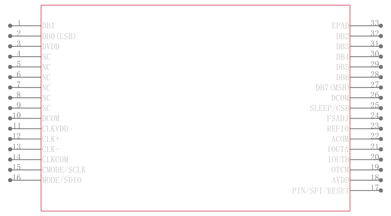
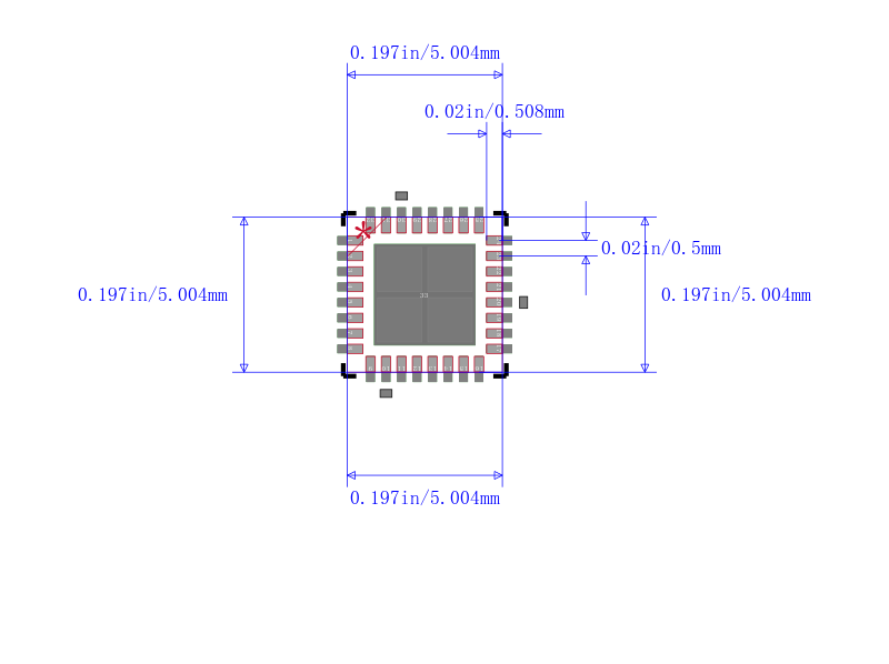
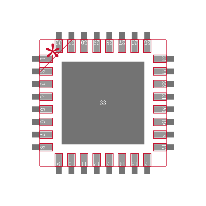
9. Industry-Standard 32-Lead LFCSP_VQ Package.
### Features and Benefits
- .
- 175 MSPS update rate
- .
- Low power member of pin-compatible
- .
- TxDAC product family
- .
- Low power dissipation
- .
- 12 mW at 80 MSPS, 1.8 V
- .
- 50 mW at 175 MSPS, 3.3 V
- .
- Wide supply voltage: 1.7 V to 3.6 V
- .
- Adjustable full-scale current outputs: 1 mA to 5 mA
- .
- On-chip 1.0 V reference
- .
- CMOS-compatible digital interface
- .
- Common-mode output: adjustable 0 V to 1.2 V
- .
- Power-down mode <2 mW at 3.3 V SPI controllable
- .
- Self-calibration
- .
- Compact 32-lead LFCSP_VQ, RoHS compliant package