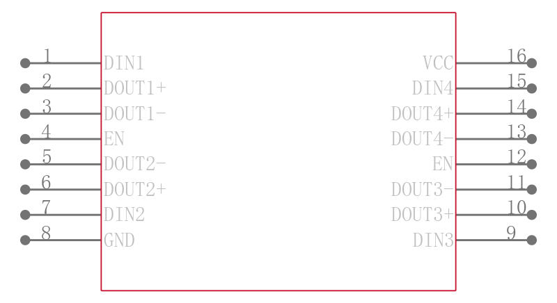
ADN4665ARUZ-REEL7
数据手册.pdf3 V , LVDS ,四通道, CMOS差分线路驱动器 3 V, LVDS, Quad, CMOS Differential Line Driver
Product Details
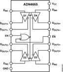
The ADN4665 is a quad-channel, CMOS, low voltage differential signaling LVDS line driver offering data rates of over 400 Mbps 200 MHz and ultralow power consumption.
The device accepts low voltage TTL/CMOS logic signals and converts them to a differential current output of typically ±3.5 mA for driving a transmission medium such as a twisted pair cable. The transmitted signal develops a differential voltage of typi-cally ±350 mV across a termination resistor at the receiving end. This voltage is converted back to a TTL/CMOS logic level by an LVDS receiver.
The ADN4665 also offers active high and active low enable/ disable inputs EN and overbar: EN. These inputs control all four drivers and turn off the current outputs in the disabled state to reduce the quiescent power consumption to typically 10 mW. The ADN4665 offers a new solution to high speed, point-to-point data transmission and offers a low power alternative to emitter-coupled logic ECL or positive emitter-coupled logic PECL.
**Applications**
* Backplane data transmission
* Cable data transmission
* Clock distribution
### Features and Benefits
- .
- ±15 kV ESD protection on output pins
- .
- 400 Mbps 200 MHz switching rates
- .
- 100 ps typical differential skew
- .
- 400 ps maximum differential skew
- .
- 2 ns maximum propagation delay
- .
- 3.3 V power supply
|
- .
- ±350 mV differential signaling
- .
- Low power dissipation 13 mW typical
- .
- Interoperable with existing 5 V LVDS receivers
- .
- High impedance on LVDS outputs on power-down
- .
- Conforms to TIA/EIA-644 LVDS standards
- .
- See data sheet for additional features
---|---