ADF5355BCPZ-RL7
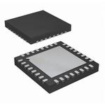
数据手册.pdfClock Generator 10MHz to 500MHz Input 14000MHz Output 32Pin LFCSP EP T/R
Product Details
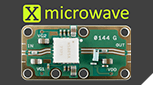
The ADF5355 allows implementation of fractional-N or integer-N phase-locked loop PLL frequency synthesizers when used with an external loop filter and an external reference frequency. The wideband microwave VCO design permits frequency operation from 6.8 GHz to 13.6 GHz at one radio frequency RF output. A series of frequency dividers at another frequency output permits operation from 54 MHz to 6800 MHz.
The ADF5355 has an integrated VCO with a fundamental output frequency ranging from 3400 MHz to 6800 MHz. In addition, the VCO frequency is connected to divide by 1, 2, 4, 8, 16, 32, or 64 circuits that allow the user to generate RF output frequencies as low as 54 MHz. For applications that require isolation, the RF output stage can be muted. The mute function is both pin and software controllable.
Control of all on-chip registers is through a simple 3-wire interface. The ADF5355 operates with analog and digital power supplies ranging from 3.15 V to 3.45 V, with charge pump and VCO supplies from 4.75 V to 5.25 V. The ADF5355 also contains hardware and software power-down modes.
**Applications**
- .
- Wireless infrastructure W-CDMA, TD-SCDMA, WiMAX, GSM, PCS, DCS, DECT
- .
- Point to point/point to multipoint microwave links
- .
- Satellites/VSATs
- .
- Test equipment/instrumentation
- .
- Clock generation
### Features and Benefits
- .
- RF output frequency range: 54 MHz to 13,600 MHz
- .
- Fractional-N synthesizer and integer-N synthesizer
- .
- High resolution 38-bit modulus
- .
- Phase frequency detector PFD operation to 125 MHz
- .
- Reference frequency operation to 600 MHz
- .
- Maintains frequency lock over −40°C to +85°C
- .
- Low phase noise, voltage controlled oscillator VCO
- .
- Programmable divide by 1, 2, 4, 8, 16, 32, or 64 output
- .
- Analog and digital power supplies: 3.3 V
- .
- Charge pump and VCO power supplies: 5.0 V, typical
- .
- Logic compatibility: 1.8 V
- .
- Programmable dual modulus prescaler of 4/5 or 8/9
- .
- Programmable output power level
- .
- RF output mute function
- .
- Analog and digital lock detect
- .
- Supported in the simPLL design tool