ADN2812ACPZ
数据手册.pdfANALOG DEVICES ADN2812ACPZ 芯片, 时钟与数据恢复器, 2.7GHZ, LFCSP-32
Product Details
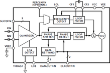
The ADN2812 provides the receiver functions of quantization, signal level detect, and clock and data recovery for continuous data rates from 12.3 Mb/s to 2.7 Gb/s. The ADN2812 automatically locks to all data rates without the need for an external reference clock or programming. All SONET jitter requirements are met, including jitter transfer, jitter generation, and jitter tolerance. All specifications are quoted for −40°C to +85°C ambient temperature, unless otherwise noted.
This device, together with a PIN diode and a TIA preamplifier, can implement a highly integrated, low cost, low power fiber optic receiver.
The receiver front end, loss of signal LOS detector circuit indicates when the input signal level has fallen below a user-adjustable threshold. The LOS detect circuit has hysteresis to prevent chatter at the output.
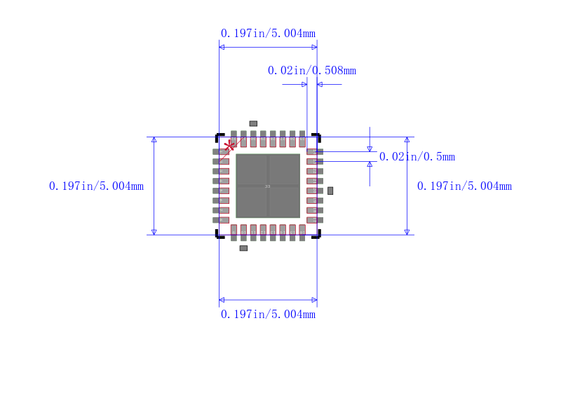
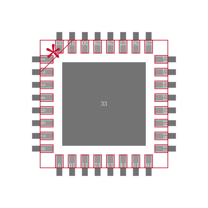
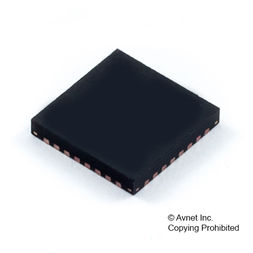
The ADN2812 is available in a compact 5 mm × 5 mm 32-lead lead frame chip scale package LFCSP.
**Applications**
- .
- SONET OC-1/OC-3/OC-12/OC-48 and all associated FEC rates
- .
- Fibre Channel, 2× Fibre Channel, GbE, HDTV
- .
- WDM transponders
- .
- Regenerators/repeaters
- .
- Test equipment
- .
- Broadband cross-connects and routers
### Features and Benefits
- .
- Serial data input: 12.3 Mb/s to 2.7 Gb/s
- .
- Exceeds SONET requirements for jitter transfer/ generation/tolerance
- .
- Quantizer sensitivity: 6 mV typical
- .
- Adjustable slice level: ±100 mV
- .
- Patented clock recovery architecture
- .
- Loss of signal LOS detect range: 3 mV to 15 mV
- .
- Independent slice level adjust and LOS detector
- .
- No reference clock required
- .
- Loss of lock indicator
- .
- I2C interface to access optional features
- .
- Single-supply operation: 3.3 V
- .
- Low power: 750 mW typical