ADN2807ACPZ-RL
数据手册.pdfCDR 155.52Mbps/166.63Mbps/622.08Mbps/666.51Mbps SONET/SDH 48Pin LFCSP EP T/R
Product Details
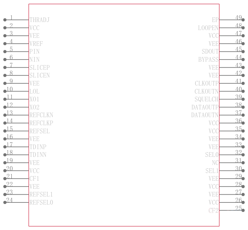
The ADN2807 provides the receiver functions of quantization, signal level detect, and clock and data recovery at rates of OC-3, OC-12, and 15/14 FEC. All SONET jitter requirements are met, including jitter transfer, jitter generation, and jitter tolerance. All specifications are quoted for –40°C to +85°C ambient temperature, unless otherwise noted.
The device is intended for WDM system applications and can be used with either an external reference clock or an on-chip oscillator with external crystal. Both native rates and 15/14 rate digital wrappers are supported by the ADN2807, without any change of reference clock.
This device, together with a PIN diode and a TIA preamplifier, can implement a highly integrated, low cost, low power, fiber optic receiver.
The receiver front end signal detect circuit indicates when the input signal level has fallen below a user adjustable threshold. The signal detect circuit has hysteresis to prevent chatter at the output.
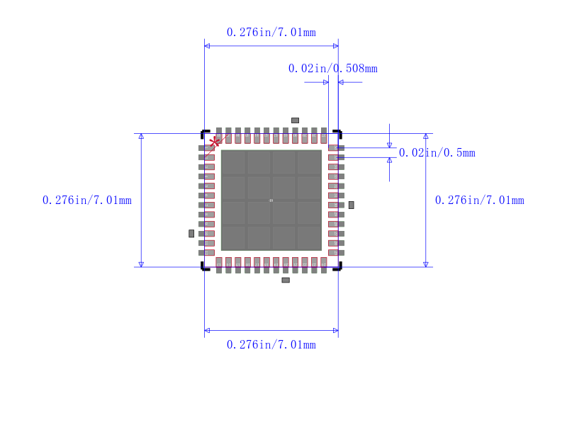
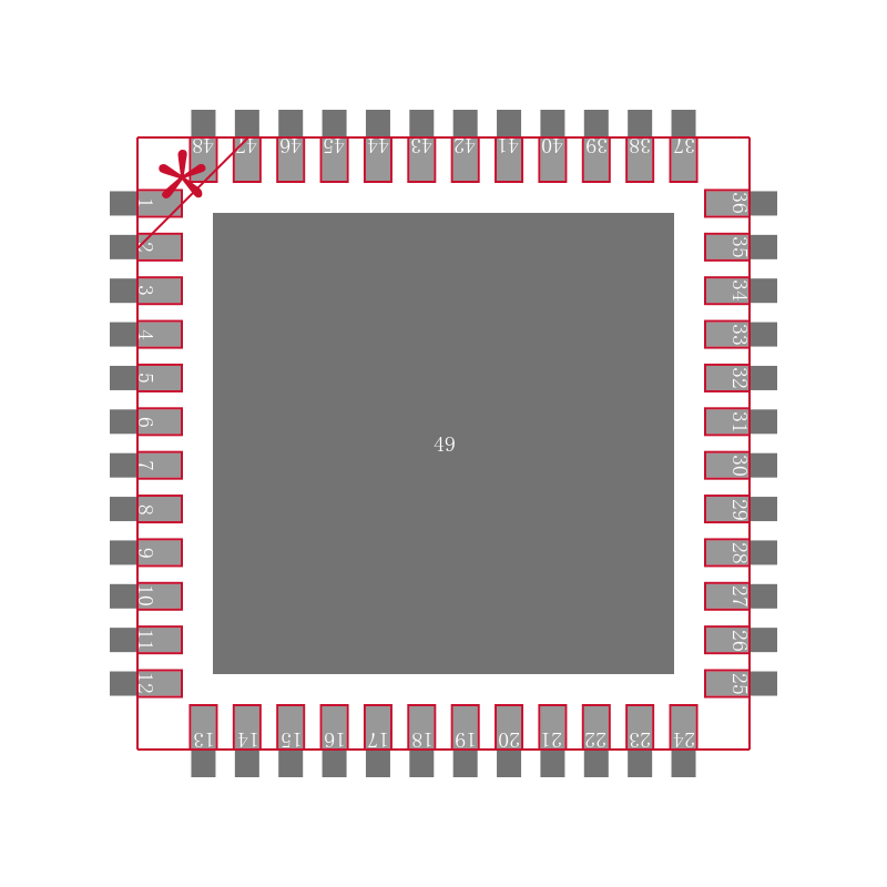
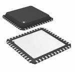
The ADN2807 is available in a compact 7 mm × 7 mm 48-lead chip-scale package LFCSP.
Applications
- .
- SONET OC-3/-12, SDH STM-1/-4 and, 15/14 FEC rates
- .
- WDM transponders
- .
- Regenerators/repeaters
- .
- Test equipment
- .
- Passive optical networks
### Features and Benefits
- .
- Meets SONET requirements for jitter transfer/generation/tolerance
- .
- Quantizer sensitivity: 4 mV typical
- .
- Adjustable slice level: ±100 mV
- .
- Patented clock recovery architecture
- .
- Loss-of-signal detect range: 3 mV to 15 mV
- .
- Single-reference clock frequency for all rates, including15/14 7% wrapper rate
- .
- Choice of 19.44 MHz, 38.88 MHz, 77.76 MHz, or 155.52 MHz REFCLK
- .
- REFCLK inputs: LVPECL/LVDS/LVCMOS/LVTTL compatible LVPECL/LVDS only at 155.52 MHz
- .
- Optional 19.44 MHz on-chip oscillator to be used with external crystal
- .
- Loss-of-lock indicator
- .
- Loopback mode for high speed test data
- .
- Output squelch and bypass features
- .
- Single-supply operation: 3.3 V
- .
- Low power: 540 mW typical
- .
- 7 mm × 7 mm, 48-lead LFCSP