AD9577BCPZ-RL
数据手册.pdf时钟发生器,提供双PLL Clock Generator with Dual PLLs
Product Details
The AD9577 provides a multioutput clock generator function, along with two on-chip phase-locked loop cores, PLL1 and PLL2, optimized for network clocking applications. The PLL designs are based on the Analog Devices, Inc., proven portfolio of high performance, low jitter frequency synthesizers to maximize network performance. The PLLs have I2C programmable output frequencies and formats. The fractional-N PLL can support spread spectrum clocking for reduced EMI radiated peak power. Both PLLs can support frequency margining. Other applications with demanding phase noise and jitter requirements can benefit from this part.
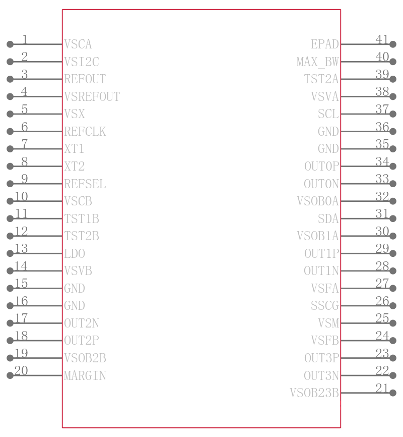
The first integer-N PLL section PLL1 consists of a low noise phase frequency detector PFD, a precision charge pump CP, a low phase noise voltage controlled oscillator VCO, a programmable feedback divider, and two independently programmable output dividers. By connecting an external crystal or applying a reference clock to the REFCLK pin, frequencies of up to 637.5 MHz can be synchronized to the input reference. Each output divider and feedback divider ratio is I2C programmed for the required output rates.
A second fractional-N PLL PLL2 with a programmable modulus allows VCO frequencies that are fractional multiples of the reference frequency to be synthesized. Each output divider and feedback divider ratio can be programmed for the required output rates, up to 637.5 MHz. This fractional-N PLL can also operate in integer-N mode for the lowest jitter.
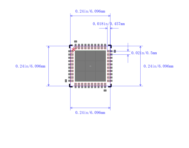
Up to four differential output clock signals can be configured as either LVPECL or LVDS signaling formats. Alternatively, the outputs can be configured for up to eight CMOS outputs. Combinations of these formats are supported. No external loop filter components are required, thus conserving valuable design time and board space. The AD9577 is available in a 40-lead, 6 mm × 6 mm LFCSP package and can operate from a single 3.3 V supply. The operating temperature range is −40°C to +85°C.
**Applications**
- .
- Low jitter, low phase noise multioutput clock generator for data communications applications including Ethernet, Fibre Channel, SONET, SDH, PCI-e, SATA, PTN, OTN, ADC/DAC, and digital video
- .
- Spread spectrum clocking
### Features and Benefits
- .
- Fully integrated dual PLL/VCO cores
- .
- 1 integer-N and 1 fractional-N PLL
- .
- Continuous frequency coverage from 11.2 MHz to 200 MHz
- .
- Most frequencies from 200 MHz to 637.5 MHz available
- .
- PLL1 phase jitter 12 kHz to 20 MHz: 460 fs rms typical
- .
- PLL2 phase jitter 12 kHz to 20 MHz
- .
- Integer-N mode: 470 fs rms typical
- .
- Fractional-N mode: 660 fs rms typical
- .
- Input crystal or reference clock frequency
- .
- Optional reference frequency divide-by-2
- .
- I2C programmable output frequencies
- .
- Up to 4 LVDS/LVPECL or up to 8 LVCMOS output clocks
- .
- 1 CMOS buffered reference clock output
- .
- Spread spectrum: downspread [0, −0.5]%
- .
- 2 pin-controlled frequency maps: margining
- .
- Integrated loop filters
- .
- Space saving, 6 mm × 6 mm, 40-lead LFCSP package
- .
- 1.02 W power dissipation LVDS operation
- .
- 1.235 W power dissipation LVPECL operation
- .
- 3.3 V operation