AD9273BSVZRL-40
数据手册.pdf模数转换器 - ADC 12-Bit 40 MSPS Octal
GENERAL DESCRIPTION
The AD9273 is designed for low cost, low power, small size, and ease of use. It contains eight channels of a low noise preamplifier LNA with a variable gain amplifier VGA; an antialiasing filter AAF; and a 12-bit, 10 MSPS to 50 MSPS analog-to digital converter ADC.
Each channel features a variable gain range of 42 dB, a fully differential signal path, an active input preamplifier termination, a maximum gain of up to 52 dB, and an ADC with a conversion rate of up to 50 MSPS. The channel is optimized for dynamic performance and low power in applications where a small package size is critical.
FEATURES
8 channels of LNA, VGA, AAF, and ADC
Low noise preamplifier LNA
Input-referred noise voltage = 1.26 nV/√Hz gain = 21.3 dB @ 5 MHz typical
SPI-programmable gain = 15.6 dB/17.9 dB/21.3 dB
Single-ended input; VIN maximum = 733 mV p-p/550 mV p-p/367 mV p-p
Dual-mode active input impedance matching
Bandwidth BW > 100 MHz
Full-scale FS output = 4.4 V p-p differential
Variable gain amplifier VGA
Attenuator range = −42 dB to 0 dB
SPI-programmable PGA gain = 21 dB/24 dB/27 dB/30 dB
Linear-in-dB gain control
Antialiasing filter AAF
Programmable 2nd-order low-pass filter LPF from 8 MHz to 18 MHz
Programmable high-pass filter HPF
Analog-to-digital converter ADC
12 bits at 10 MSPS to 50 MSPS
SNR = 70 dB
SFDR = 75 dB
Serial LVDS ANSI-644, IEEE 1596.3 reduced range link
Data and frame clock outputs
Includes an 8 × 8 differential crosspoint switch to support continuous wave CW Doppler
Low power, 109 mW per channel at 12 bits/40 MSPS TGC
70 mW per channel in CW Doppler
Flexible power-down modes
Overload recovery in <10 ns
Fast recovery from low power standby mode, <2 μs
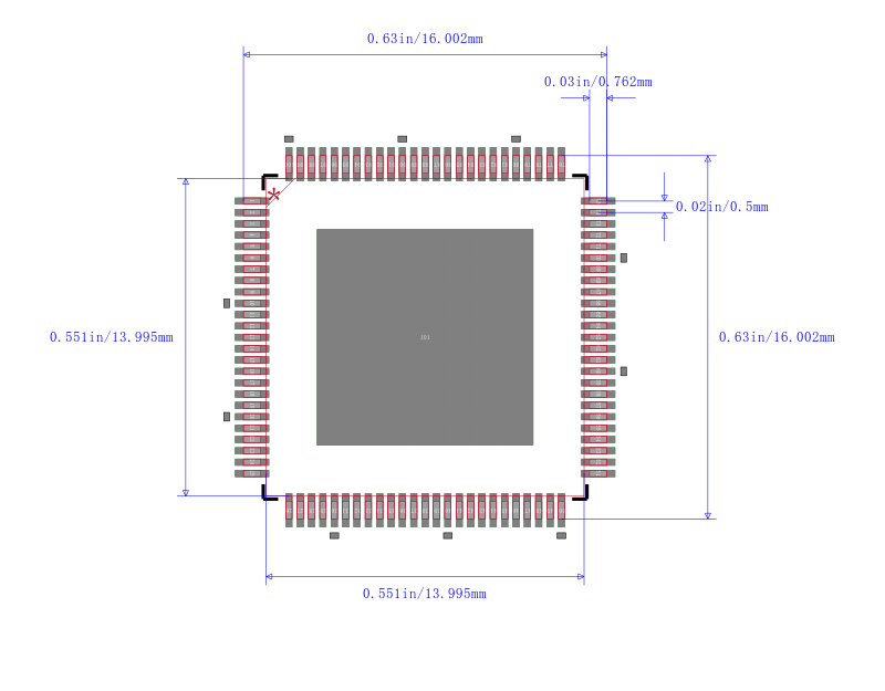
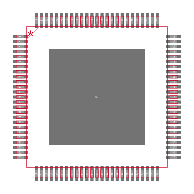
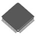
100-lead TQFP and 144-ball BGA
APPLICATIONS
Medical imaging/ultrasound
Automotive radar