ADG5213BCPZ-RL7
数据手册.pdfANALOG DEVICES ADG5213BCPZ-RL7 模拟开关, 四通道, SPST, 4 放大器, 200 ohm, 9V 至 40V, ± 9V 至 ± 22V, LFCSP, 16 引脚
Product Details
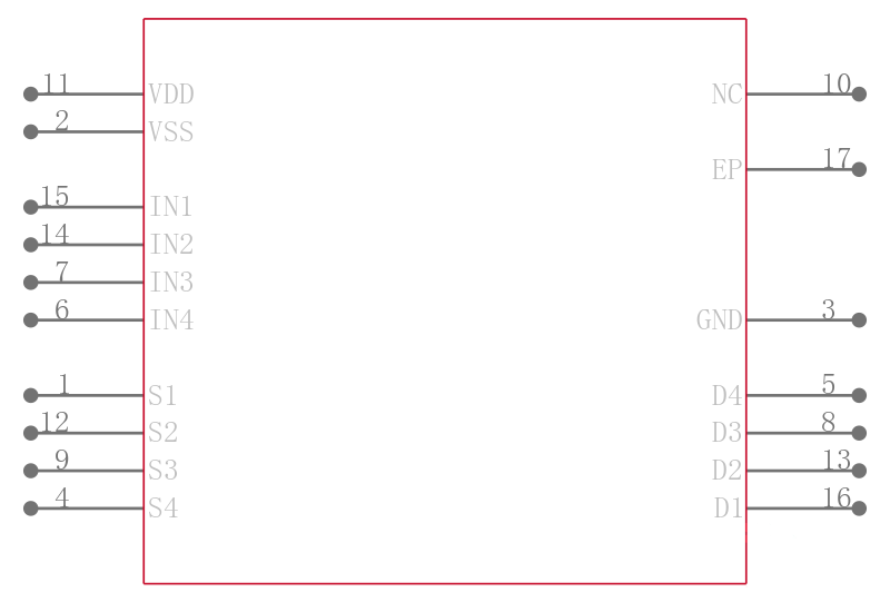
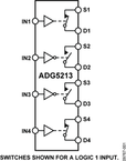
The ADG5212/ADG5213 contain four independent single-pole/single-throw SPST switches. The ADG5212 switches turn on with Logic 1. The ADG5213 has two switches with digital control logic similar to that of the ADG5212; however, the logic is inverted on the other two switches. Each switch conducts equally well in both directions when on, and each switch has an input signal range that extends to the supplies. In the off condition, signal levels up to the supplies are blocked.
The ADG5212 and ADG5213 do not have a VL pin. The digital inputs are compatible with 3 V logic inputs over the full operating supply range.
The ultralow capacitance and charge injection of these switches make them ideal solutions for data acquisition and sample-and-hold applications, where low glitch and fast settling are required. Fast switching speed together with high signal bandwidth make the parts suitable for video signal switching.
**APPLICATIONS**
- .
- Automatic test equipment
- .
- Data acquisition
- .
- Instrumentation
- .
- Avionics
- .
- Audio and video switching
- .
- Communication systems
**Product Highlights**
1. Trench Isolation Guards Against Latch-Up.
A dielectric trench separates the P and N channel transistors thereby preventing latch-up even under severe overvoltage conditions.
2. Ultralow capacitance and < 1 pC charge injection.
3. Dual-Supply Operation.
For applications where the analog signal is bipolar, the ADG5212/ADG5213 can be operated from dual supplies up to ±22V.
4. Single-Supply Operation.
For applications where the analog signal is unipolar, the ADG5212/ADG5213 can be operated from a single rail power supply up to 40 V.
5. 3 V Logic Compatible Digital Inputs.
VINH = 2.0 V, VINL = 0.8 V.
6. No VL Logic Power Supply Required.
### Features and Benefits
- .
- Latch-up proof
- .
- 3 pF off source capacitance
- .
- 5 pF off drain capacitance
- .
- 0.07 pC charge injection
- .
- Low leakage: 0.2 nA maximum at 85ºC
- .
- ±9 V to ±22 V dual-supply operation
- .
- 9 V to 40 V single-supply operation
- .
- 48 V supply maximum ratings
- .
- Fully specified at ±15 V, ±20 V, +12 V, and +36 V
- .
- VSS to VDD analog signal range