DTA115EET1
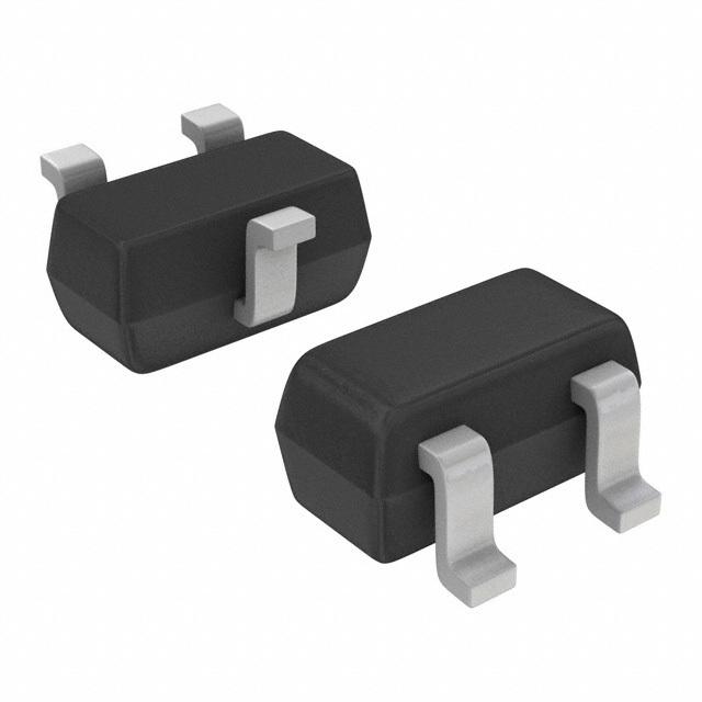
数据手册.pdfDTA115EET1 带阻尼PNP三极管 -50V -20mA 0.15W/150mW SOT-523/SC-75 标记6N 开关电路,逆变器,接口电路,驱动电路
集电极-基极反向击穿电压VBRCBO Collector-Base VoltageVCBO| -50V \---|--- 集电极-发射极反向击穿电压VBRCEO Collector-Emitter VoltageVCEO| -50V 集电极连续输出电流IC Collector CurrentIC| -20mA 基极输入电阻R1 Input ResistanceR1| 100KΩ/Ohm 基极-发射极输入电阻R2 Base-Emitter ResistanceR2| 100KΩ/Ohm 电阻比R1/R2 Resistance Ratio| 1 直流电流增益hFE DC Current GainhFE| 截止频率fT Transtion FrequencyfT| 250MHz 耗散功率Pc Power Dissipation| 0.15W/150mW Description & Applications| Feature •Digital transistors built-in resistor •Built-in bias resistors enable the configuration of an inverter circuit without connecting external input resistors see equivalent circuit. •The bias resistors consist of thin-film resistors with complete isolation to allow positive biasing of the input. They also have the advantage of almost completely eliminating parasitic effects. •Only the on/off conditions need to be set for operation, making device design easy •Higher mounting densities can be achieved. 描述与应用| 特点 •数字(内置电阻) •内置启用偏置电阻器的逆变器电路的配置,而无需连接外部输入电阻(见等效电路)。 •偏置电阻组成的薄膜电阻完全隔离,允许输入的正偏压。他们也有优势,几乎完全消除了寄生效应。 •只有开/关条件需要设置操作,使装置的设计容易 •高密度安装就可以实现。